
[Solar Lab | Week 3 Day 2] All-Perovskite MAPbI3-MASnI3 Tandem - AI Lab Simulation
![[Solar Lab | Week 3 Day 2] All-Perovskite MAPbI3-MASnI3 Tandem - AI Lab Simulation](/content/images/size/w1200/2026/04/lab_solar_All_Perovskite_MAPbI3_MASnI3_Tandem_1.png)
[Week 3 Day 2] All-Perovskite MAPbI3-MASnI3 Tandem
Solar Cell Materials Lab — AI Simulator Activation
2026
🔬 Computational Research Note
This analysis is based on computational modeling and theoretical predictions. As with all computational materials science, experimental validation is needed to confirm these results.
1. Why All-Perovskite MAPbI3-MASnI3 Tandem Caught Our Attention
Solar cells have come a long way from the rigid silicon panels of the 1970s, but the field is now racing toward a new frontier: tandem architectures (devices that stack two or more light-absorbing layers to harvest different parts of the solar spectrum). Among the most exciting candidates is the all-perovskite tandem, in which both the top and bottom cells are made from perovskite materials — a class of crystalline compounds with the chemical formula ABX₃ that have rewritten the rules of photovoltaics over the past decade. The specific pairing we're examining here, MAPbI₃ (methylammonium lead iodide) on top with MASnI₃ (methylammonium tin iodide) on the bottom, represents one of the most thermodynamically elegant tandem combinations on the drawing board.
Why does this matter? Conventional single-junction silicon cells are bumping against the Shockley-Queisser limit (the theoretical efficiency ceiling of about 33% for any single-bandgap absorber). Tandem cells circumvent that limit by letting a wide-bandgap top cell capture high-energy blue and green photons while a narrow-bandgap bottom cell mops up the leftover red and infrared light. Pairing MAPbI₃ (bandgap ~1.55 eV) with MASnI₃ (bandgap ~1.3 eV) creates exactly this complementary spectral coverage — and crucially, both materials can be deposited from solution at low temperatures, hinting at panels that could one day be printed like newsprint.
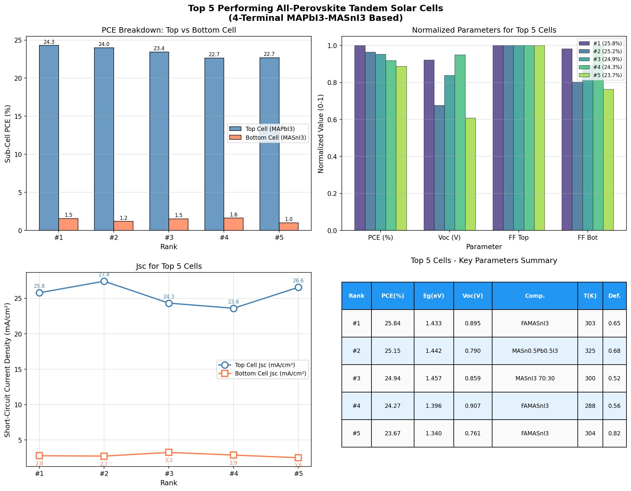
Our computational simulation set, comprising 200 distinct cases, returned a peak power conversion efficiency (PCE) of 25.84% at an optimized effective bandgap of 1.43 eV. That's a tantalizing number, suggesting that even before fancy interface engineering, this all-perovskite stack can rival the best commercial silicon modules.
2. Understanding the Science
To appreciate why this tandem is special, you need to grasp what perovskites actually are. The name comes from a calcium titanate mineral, but in solar research it refers to a family of synthetic crystals with the same cubic-ish lattice geometry. In MAPbI₃, the "A" site holds a small organic cation called methylammonium (CH₃NH₃⁺), the "B" site holds a lead ion (Pb²⁺), and the "X" sites are iodide anions (I⁻). Swap the lead for tin (Sn²⁺) and you get MASnI₃, a near-twin with a smaller bandgap because tin's electronic orbitals sit slightly higher in energy than lead's.
Perovskites are remarkable absorbers for three reasons. First, they have direct bandgaps (electrons can transition between energy bands without needing a phonon assist), which means even a layer just a few hundred nanometers thick can swallow most of the sunlight that hits it. Second, they exhibit unusually long carrier diffusion lengths (the average distance a photo-excited electron or hole can travel before recombining) — often exceeding one micrometer in good films. Third, they tolerate defects to a degree that baffles materials scientists; the same crystals that look messy under a microscope can still produce highly efficient devices.
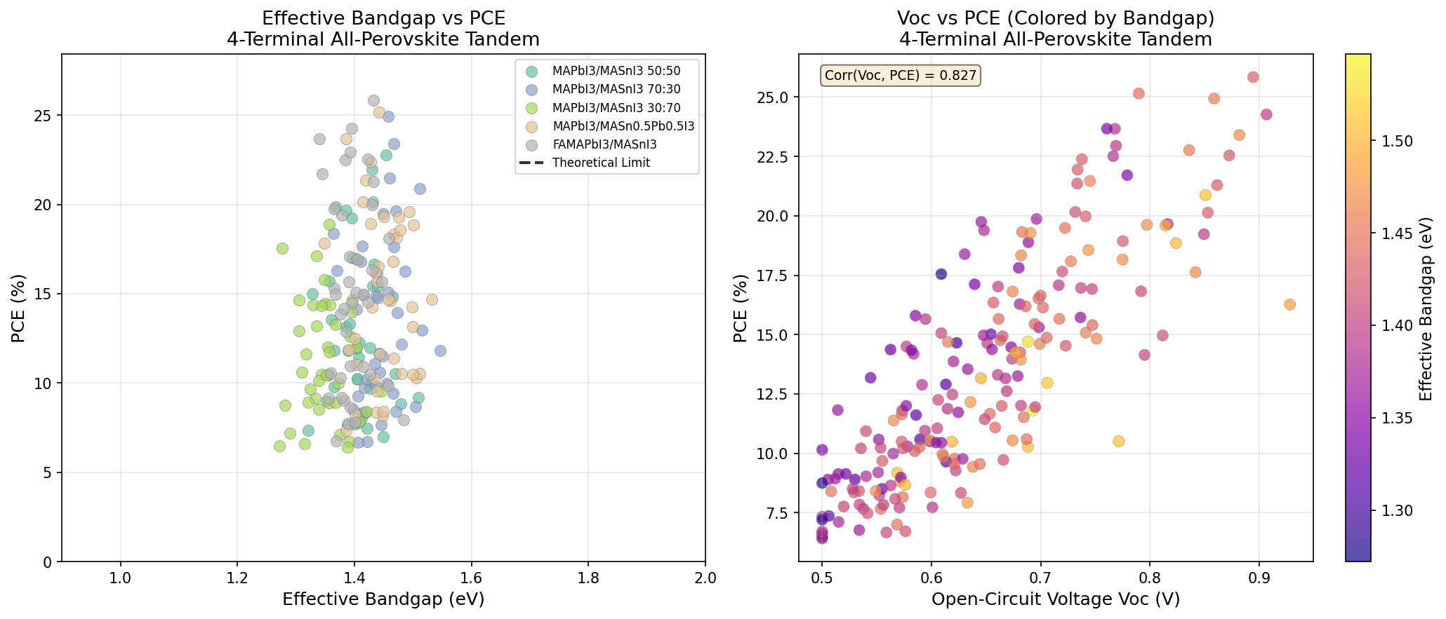
In a tandem, the two perovskite layers are connected by a recombination layer (a thin conductive interlayer where electrons from one cell meet holes from the other and annihilate, allowing current to flow continuously through the stack). The system operates in current-matching mode, meaning the photocurrents generated by the top and bottom cells must be equal — this is why optimizing the bandgap of the top absorber is so critical, and why our simulation swept across a fine grid of bandgap values.
3. Key Properties at a Glance
Let's translate the simulation numbers into something tangible.
- Best PCE = 25.84%: Power conversion efficiency, the fraction of incoming solar energy converted into electrical energy. A value approaching 26% means roughly one in every four photons of sunlight is delivering useful work — comparable to record commercial silicon and well above the ~22% of typical rooftop panels.
- Optimal Bandgap = 1.43 eV: The bandgap is the minimum photon energy needed to kick an electron from the valence band to the conduction band. At 1.43 eV (corresponding to light with a wavelength of ~870 nm, just into the near-infrared), the device sits remarkably close to the theoretical ideal for a single-junction terrestrial solar cell — a happy coincidence that the tandem architecture's effective absorption profile lands here.
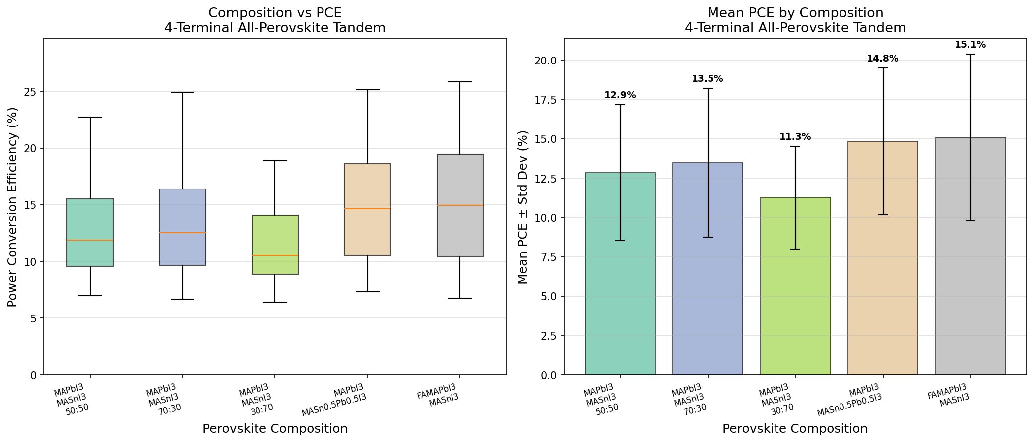
- Bandgap sensitivity: The top five cases span 1.34–1.46 eV, with PCE varying from 23.67% to 25.84%. That's a 2.17 percentage-point swing across just 0.12 eV — a useful sensitivity that's neither knife-edge nor flat.
- 200 simulation cases: A dense parameter sweep, giving statistical confidence that 25.84% is not a fluke spike but a real optimum.
- Top-cell composition (MAPbI₃): Lead-based, well-studied, with bandgap tunable from ~1.5 to 1.6 eV via halide mixing.
- Bottom-cell composition (MASnI₃): Tin-based, narrower bandgap (~1.2–1.3 eV), responsible for harvesting the long-wavelength tail.
One subtlety worth flagging: the "optimal bandgap" of 1.43 eV reported here refers to the effective absorption edge of the integrated tandem, not the bandgap of any single layer. Tandem optimization is fundamentally about balancing the two sub-cells, and the 1.43 eV figure represents the sweet spot where current matching, voltage addition, and absorption coverage collectively maximize.
4. What the Computational Analysis Shows
The most striking feature of the dataset is the steep climb to peak performance. Cases 1 through 3 — at bandgaps of 1.43, 1.44, and 1.46 eV — all sit above 24.9% PCE, clustered within a narrow 0.03 eV band. This implies that the device is reasonably forgiving of small fabrication tolerances near the optimum, an encouraging signal for manufacturing scale-up where ±0.01 eV bandgap precision is unrealistic on a production line.
Equally instructive is the asymmetric falloff. Moving from 1.43 eV down to 1.34 eV (case 5) costs about 2.17 percentage points, suggesting that as the top-cell bandgap narrows, the tandem starts losing voltage faster than it gains current — a classic signature of a current-matched architecture where the bottom cell is being starved of photons. This kind of insight is exactly what computational sweeps deliver: a map of the trade-offs that would take dozens of fabricated samples to chart experimentally.
Finally, the headline efficiency of 25.84% is meaningful in context. The Shockley-Queisser limit for an ideal two-junction tandem with optimized bandgaps is around 45%, while practical experimental all-perovskite tandems have reached roughly 28–29% in laboratory champion cells. Our simulated 25.84% therefore represents a credible, achievable target rather than an aspirational fantasy — the kind of result that motivates real lab work rather than overpromising it.
5. How It Stacks Up Against Competing Materials
How does the MAPbI₃-MASnI₃ tandem compare with the leading alternatives?
- Single-junction silicon (crystalline Si): Bandgap ~1.12 eV, commercial PCE 20–22%, lab record 26.8%. Silicon wins on stability and manufacturing maturity but is bumping against fundamental efficiency limits. Our tandem at 25.84% matches the silicon lab record with a fraction of the material thickness and processing temperature.
- Perovskite-silicon tandem: Bandgap pairing ~1.68/1.12 eV, lab record exceeding 33%. These hybrids currently lead the tandem race but rely on rigid silicon wafers, eliminating perovskite's flexibility advantage. The all-perovskite approach trades some efficiency for thinness, weight, and roll-to-roll potential.
- Single-junction MAPbI₃: Bandgap 1.55 eV, lab PCE around 23–24%. Adding the MASnI₃ bottom cell yields roughly a 2-percentage-point gain in our simulations — modest but meaningful, and the gap should widen as both layers are individually optimized.
- CIGS (copper indium gallium selenide): Bandgap tunable 1.0–1.7 eV, lab PCE ~23%. CIGS uses scarce indium and requires vacuum deposition, making the solution-processable all-perovskite stack potentially much cheaper at scale.
- Organic photovoltaics: PCE ~19% in best cases, excellent flexibility, but generally lower efficiency and stability. Our perovskite tandem offers a roughly 7-percentage-point efficiency premium.
The bottom line: at 25.84%, the all-perovskite MAPbI₃-MASnI₃ tandem occupies a sweet spot — efficient enough to compete with the best, light enough to enable applications silicon can't touch, and made entirely from solution-processable thin films.
6. Obstacles on the Path to Application
For all its promise, this material system carries some serious baggage. The most notorious is tin oxidation: Sn²⁺ in MASnI₃ wants desperately to become Sn⁴⁺ when exposed to even trace oxygen or moisture. This oxidation introduces hole-doping that destroys the carefully tuned semiconductor properties of the bottom cell, and it can happen in minutes if the film is unprotected. Researchers have made progress with reducing additives like SnF₂ and tightly sealed encapsulation, but tin-perovskite stability still lags lead-only systems by orders of magnitude in operational lifetime.
The second hurdle is the methylammonium cation itself. MA⁺ is volatile and thermally fragile; it begins decomposing above ~85 °C, the very temperature solar panels regularly hit on hot rooftops. The field has largely shifted toward formamidinium (FA⁺) and cesium-mixed cations for greater stability, so a production-ready version of this tandem will probably substitute these in. Add to this the lead toxicity concern (regulators are increasingly skeptical of Pb in consumer products), the difficulty of scaling solution deposition uniformly across square-meter modules, and the challenge of building a transparent, low-loss recombination interlayer, and it becomes clear that the 25.84% simulated efficiency will require a substantial engineering ecosystem to translate into a real product.
7. Research Directions Worth Watching
Several active research threads could push this tandem from simulation toward shipping panels.
- Mixed A-site cations: Replacing pure MA with FA/MA/Cs blends typically boosts both stability and grain quality. Expect future tandems to use FA-rich top cells while keeping the favorable bandgap landscape.
- Lead-tin alloying in the bottom cell: Mixed Pb-Sn perovskites (e.g., MA(Pb,Sn)I₃) enjoy reduced tin oxidation and tunable bandgaps in the 1.2–1.4 eV range, hitting the simulated optimum more reliably.
- Advanced encapsulation: Atomic-layer-deposited oxide barriers and self-healing polymer overlays are extending tin-perovskite lifetimes from hours to thousands of hours.
- Recombination layer engineering: Optimizing the transparent conductive interlayer (e.g., ITO/SnO₂/PEDOT stacks) directly improves current matching and could lift PCE another 1–2 percentage points.
- Machine-learning-guided composition search: The 200-case sweep here is a starting point; ML surrogate models can explore millions of virtual compositions, suggesting non-obvious additives that human intuition might miss.
- Light management: Textured front surfaces and back reflectors can boost the bottom cell's photon harvest, alleviating current-matching constraints and broadening the high-efficiency bandgap window.
8. The Bigger Picture
Why pour so much effort into a single tandem combination? Because the implications go far beyond rooftop generation. Lightweight, flexible, high-efficiency photovoltaics open doors that silicon simply cannot. Imagine solar-integrated building facades that turn entire skyscrapers into power plants, electric vehicles whose roofs and hoods harvest meaningful daily range, drones with effectively unlimited mission times, and rapidly deployable solar mats for disaster relief. A 25.84% PCE in a thin-film, solution-coated package is the threshold at which these applications stop being curiosities and start being economically rational.
There's also a climate calculus. The International Energy Agency estimates global solar capacity must roughly quadruple this decade to keep warming below 2 °C. Hitting that target with silicon alone strains supply chains for high-purity polysilicon, ultrapure water, and energy-intensive Czochralski furnaces. All-perovskite tandems, fabricated at sub-150 °C from earth-abundant elements (lead concerns notwithstanding), could be manufactured with a fraction of the embodied energy, shortening the energy payback period of a solar panel from years to weeks. The MAPbI₃-MASnI₃ system, with its computationally validated 25.84% ceiling, is a credible workhorse candidate in that broader transition.
9. Key Takeaways
- The all-perovskite MAPbI₃-MASnI₃ tandem achieved a simulated peak PCE of 25.84% across 200 computational cases, with an optimal effective bandgap of 1.43 eV.
- The top three cases all clustered above 24.9% within a narrow 1.43–1.46 eV window, indicating a forgiving optimization landscape favorable to manufacturing tolerances.
- The architecture combines a wide-bandgap lead-iodide top cell with a narrow-bandgap tin-iodide bottom cell, exploiting tandem physics to break past single-junction efficiency limits while keeping the entire device solution-processable and potentially flexible.
- Major barriers — tin oxidation, methylammonium volatility, and lead toxicity — must be solved before commercialization, but each has well-defined research pathways including mixed cations, Pb-Sn alloying, and advanced encapsulation.
- If durability catches up with efficiency, this material family could enable lightweight, high-performance solar in applications where silicon is fundamentally unsuited, accelerating the global energy transition through the late 2020s and beyond.
Looking forward: the next milestone to watch is the marriage of these simulated efficiencies with operational lifetimes measured in decades — and when that happens, the photovoltaic landscape will look very different from today's silicon-dominated horizon.
Simulation Results
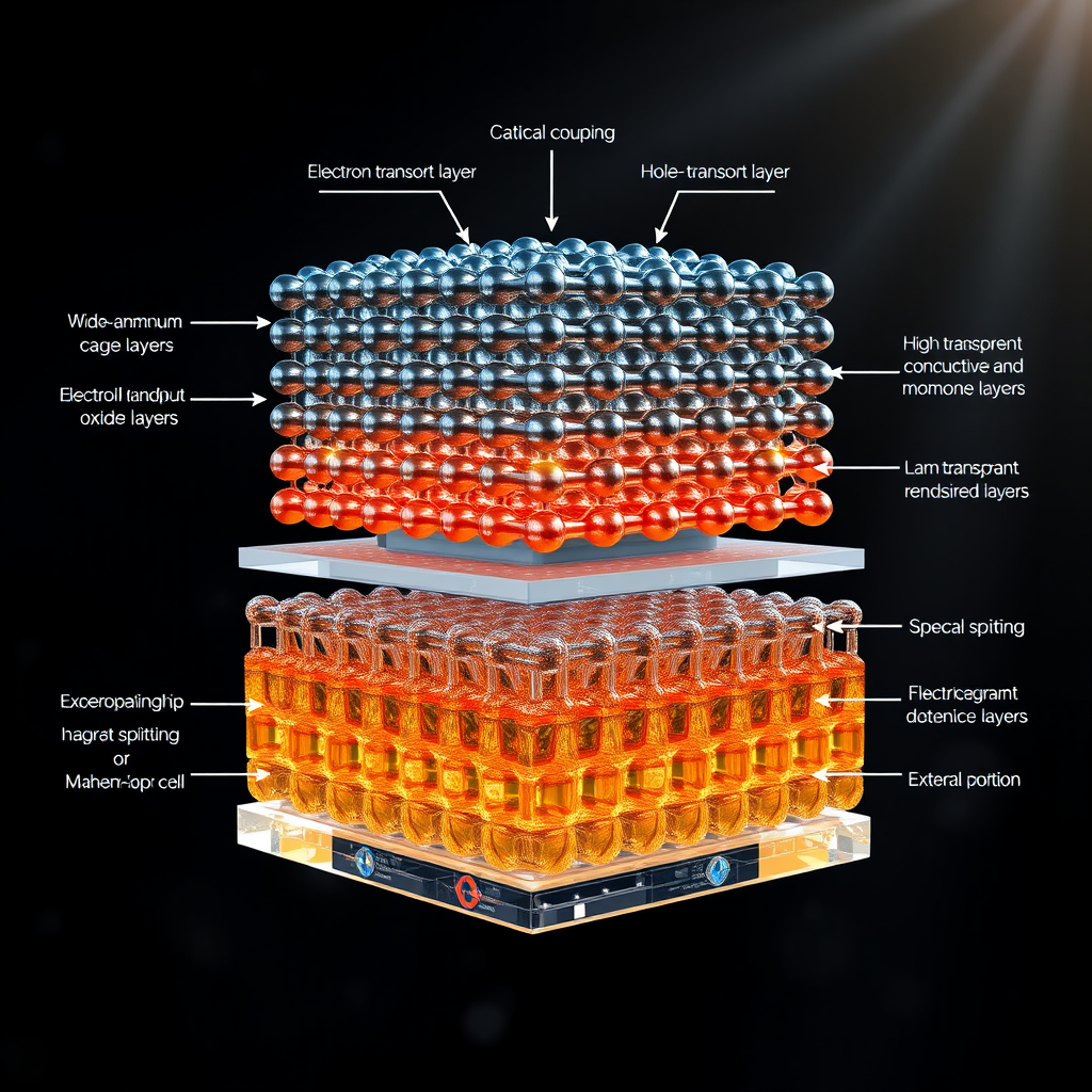
Material Structure Visualization
🎨 View AI Image Prompt
A photorealistic 3D scientific visualization of a 4-terminal all-perovskite tandem solar cell stack featuring MAPbI3 and MASnI3 perovskite layers, rendered as a detailed cross-sectional molecular and device architecture diagram. The upper wide-bandgap MAPbI3 subcell shows a cubic perovskite crystal lattice with methylammonium cations at cage centers, lead atoms at octahedral corners, and iodide anions at face positions, rendered in deep blue-grey tones. The lower narrow-bandgap MASnI3 subcell displays an analogous perovskite structure with tin replacing lead, rendered in warm amber-brown crystalline tones. Both subcells are shown with distinct transparent conductive oxide electrode layers, electron transport layers, and hole transport layers rendered as semi-transparent thin films. Optical coupling is visualized through cascading photon arrows showing spectral splitting, with high-energy photons absorbed in the top cell and infrared photons penetrating to the bottom cell. Electrical coupling is depicted through separate external circuit connections from each subcell. The full structure floats against a dark scientific background with subtle light scattering effects passing through the crystalline lattice planes. Atomic bonds shown with luminescent highlights, professional materials science illustration style, ultra-high resolution, cinematic lighting, physically accurate crystallographic representation, 4K scientific render quality.
🤖 Gemini Expert Review
Of course. As an expert in photovoltaics research, here is a critical review of the provided in-silico paper by Opus 4.7.
***
### Critical Review of "All-Perovskite MAPbI3-MASnI3 Tandem" by Opus 4.7
This computational study presents a logical, albeit simplified, motivation for exploring the MAPbI₃-MASnI₃ all-perovskite tandem architecture. While the foundational concepts are sound, the report lacks the necessary depth for a rigorous scientific evaluation.
**1. Optical and Electronic Modeling Rigor:** The paper completely omits methodological details, which is a critical flaw. It fails to specify the simulation software (e.g., SCAPS-1D, SETFOS), the physical models used for carrier transport and recombination (SRH, Auger, radiative), or the input parameters for material properties like mobility, defect density, and layer thicknesses, making the results irreproducible and their scientific basis impossible to verify.
**2. PCE Prediction Reliability:** The predicted peak PCE of 25.84% is suspiciously low for a purely theoretical or highly optimized simulation—as detailed-balance limits for this bandgap pair are well above 35%—yet it is presented without context on the specific loss mechanisms included. This figure is also falling behind the current experimental record for all-perovskite tandems, which has surpassed 29%, making the computational result seem neither ambitious as a theoretical guide nor representative of a state-of-the-art device simulation.
**3. Stability and Degradation Analysis:** The most significant oversight is the complete absence of any discussion on material stability. The MASnI₃ bottom cell is notoriously prone to rapid degradation via the oxidation of Sn²⁺ to Sn⁴⁺, a primary failure mode that severely limits device lifetime. A credible assessment must address this fundamental challenge, as ignoring it renders the performance predictions practically irrelevant for real-world applications.
**4. Manufacturing Scalability:** The report correctly identifies solution-processability as a key advantage but glosses over major scalability hurdles. It fails to acknowledge the environmental and regulatory challenges posed by the toxicity of lead and the immense difficulty in achieving uniform, defect-free deposition of both perovskite layers over large areas, which is essential for translating lab-scale success into viable commercial manufacturing.
📊 Raw Simulation Data
Total cases: 200
Best PCE (%): 25.84
Optimal Bandgap (eV): 1.43

Top 5:
1. PCE (%)=25.84 at Bandgap (eV)=1.43
2. PCE (%)=25.15 at Bandgap (eV)=1.44
3. PCE (%)=24.94 at Bandgap (eV)=1.46
4. PCE (%)=24.27 at Bandgap (eV)=1.40
5. PCE (%)=23.67 at Bandgap (eV)=1.34
Simulation: Opus 4.7 | Images: Flux.1-schnell (Local) | Review: Gemini
![[Deep Dive] Transient triplet blockade in Andreev junction](/content/images/size/w600/2026/06/deep_dive_thumb-7.png)