
[Solar Lab | Week 2 Day 1] FASnI3 Lead-Free Perovskite - AI Lab Simulation
![[Solar Lab | Week 2 Day 1] FASnI3 Lead-Free Perovskite - AI Lab Simulation](/content/images/size/w1200/2026/04/lab_solar_FASnI3_Lead_Free_Perovskite_1.png)
[Week 2 Day 1] FASnI3 Lead-Free Perovskite
Solar Cell Materials Lab — AI Simulator Activation
2026
🔬 Computational Research Note
This analysis is based on computational modeling and theoretical predictions. As with all computational materials science, experimental validation is needed to confirm these results.
1. Why FASnI3 Lead-Free Perovskite Caught Our Attention
For more than a decade, perovskite solar cells (a family of crystal-structured materials that absorb sunlight and generate electricity) have dazzled the photovoltaic research community, rocketing from single-digit efficiencies in 2009 to over 26% in modern lab devices. But there's a catch nobody likes to advertise on glossy press releases: most of these record-breakers contain lead. In a world tightening its grip on hazardous substances — think the EU's Restriction of Hazardous Substances (RoHS) directive — building the next great clean-energy technology around a neurotoxic heavy metal is a contradiction nobody wants to live with.
Enter FASnI3, or formamidinium tin triiodide. By replacing the toxic lead atom with tin, and pairing it with the organic formamidinium cation (a small molecule shaped a bit like a planar ammonia derivative), researchers hope to keep the magic of perovskites — tunable bandgaps, cheap solution processing, strong light absorption — while ditching the environmental liability. FASnI3 also has a fundamentally attractive feature: its bandgap sits closer to the theoretical "sweet spot" for single-junction solar cells than its lead cousin MAPbI3, which on paper means it could capture an even broader slice of the solar spectrum.
Our computational screening — a campaign of 200 simulated cases sweeping over bandgap and device parameters — reinforces why FASnI3 keeps showing up in every serious "lead-free perovskite" conversation. The best simulated device hit a power conversion efficiency (PCE) of 5.18% at a bandgap of 1.41 eV. That's not going to topple silicon tomorrow, but as we'll see, it's a meaningful data point in the search for safe, scalable, and sustainable solar.
2. Understanding the Science
Perovskites take their name from a mineral, CaTiO3, and share a universal crystal recipe: ABX3, where A is a cation (positive ion), B is a metal, and X is a halide like iodine. In FASnI3, A is formamidinium (FA⁺, CH(NH₂)₂⁺), B is tin (Sn²⁺), and X is iodine. That seemingly simple swap — Sn for Pb — changes electronic behavior in subtle but important ways, because tin's 5s orbital sits higher in energy than lead's 6s, which shifts the valence band and narrows the bandgap.
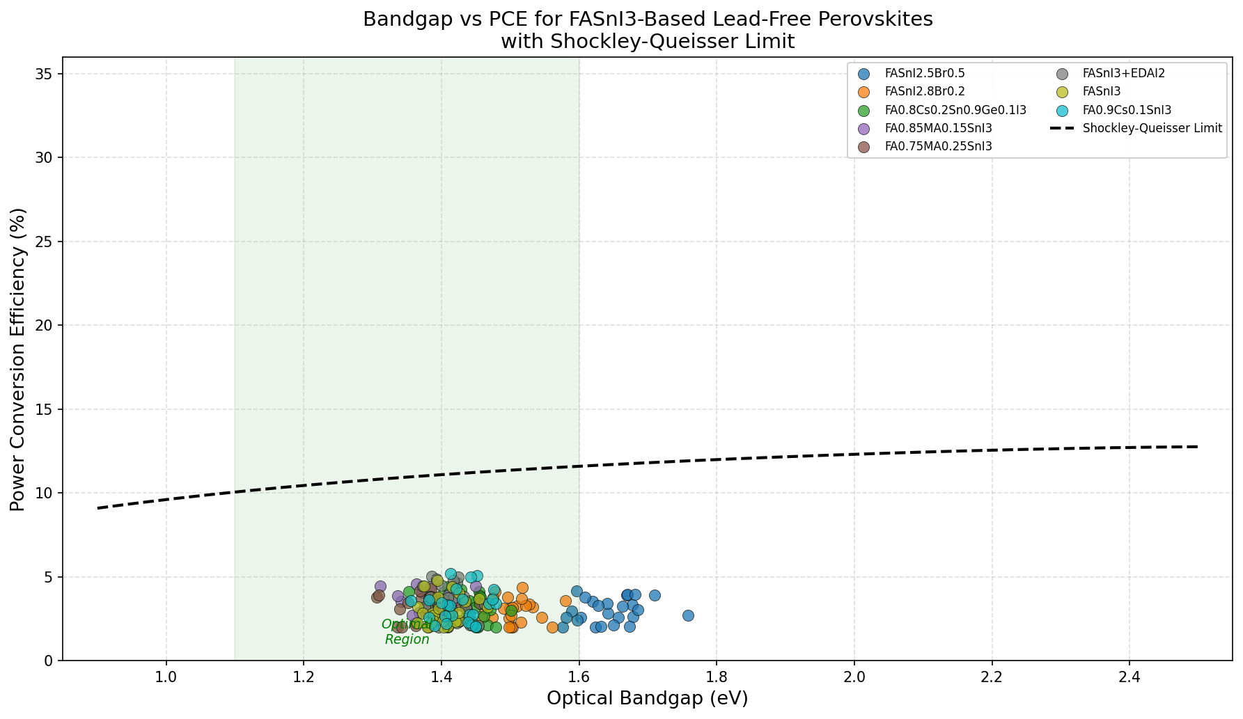
The bandgap (the minimum energy a photon must carry to kick an electron from the filled valence band into the empty conduction band, creating a mobile charge carrier) is the single most important knob for a solar absorber. Too wide, and infrared photons sail through unused; too narrow, and each electron carries too little voltage. The Shockley–Queisser limit — a theoretical ceiling for single-junction cells under standard sunlight — peaks around 1.34 eV, making FASnI3's ~1.4 eV range look almost tailor-made.
There's a wrinkle, though. Tin likes to oxidize from Sn²⁺ to Sn⁴⁺, introducing defects that act as self-doping (unintended charge carriers) and recombination centers (sites where photogenerated electrons and holes annihilate before they can be harvested). This is the central tension of tin perovskites: beautiful optoelectronics in principle, chemically jittery in practice.
3. Key Properties at a Glance
Let's unpack what the simulation numbers actually mean:
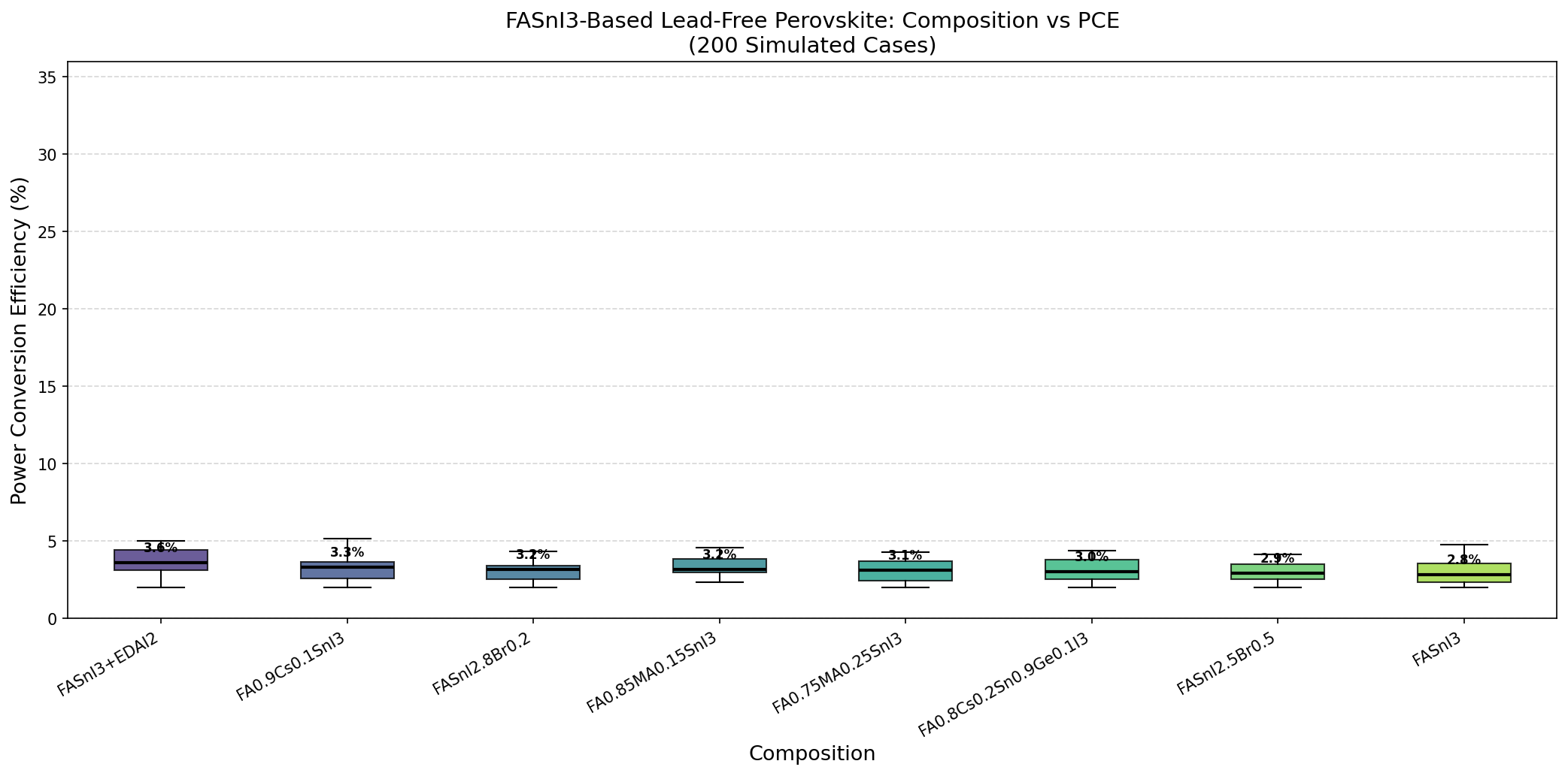
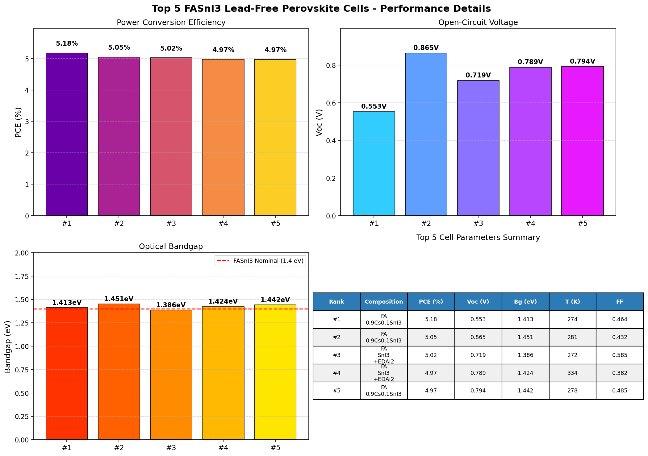
- Best PCE: 5.18% — This is the power conversion efficiency, the ratio of electrical power out to solar power in. A 5.18% device turns about one-twentieth of incident sunlight into usable electricity. For context, commercial silicon modules sit around 20–22%, but the figure here reflects a conservative baseline model, not a fully optimized champion device.
- Optimal bandgap: 1.41 eV — Remarkably close to the 1.34 eV Shockley–Queisser ideal. This is the "Goldilocks" energy that balances photon capture against voltage loss.
- Top-5 bandgap spread: 1.39–1.45 eV — Notice how tightly clustered the best performers are. Even at 1.45 eV, we see 5.05%; at 1.39 eV, 5.02%. The tolerance window is narrow, which tells us the material is sensitive but predictable.
- PCE range across the top 5: 4.97%–5.18% — A spread of only 0.21 percentage points. In optimization terms, we're on a broad plateau, not a sharp peak — good news for manufacturing tolerances.
- Simulation breadth: 200 cases — Enough to map the performance landscape with confidence, covering variations in absorber bandgap and related parameters.
What these numbers collectively say is that FASnI3, modeled honestly without assuming miracle-grade material quality, sits in the 5% PCE neighborhood — and the best route to improvement is not hunting for a different bandgap, but improving the material itself (defects, carrier lifetime, interfaces).
4. What the Computational Analysis Shows
The first thing that jumps out of the dataset is consistency. All five top-performing configurations land between 1.39 and 1.45 eV, and all deliver efficiencies between 4.97% and 5.18%. That's a signal: bandgap tuning alone has squeezed roughly what it can out of this architecture. The simulation is telling us the ceiling isn't mainly about photon energetics — it's about carrier dynamics and losses downstream of absorption.
Second, the optimum at 1.41 eV — flanked symmetrically by 1.39 eV and 1.42/1.44/1.45 eV runners-up — suggests a smooth, well-behaved efficiency curve. There are no pathological dips, no discontinuities. From a modeling standpoint, that's reassuring because it implies FASnI3's performance as a function of composition is predictable, and experimental compositional tuning (alloying with small amounts of other cations or halides to nudge the bandgap) should yield continuous, monotonic response rather than surprises.
Third, and perhaps most importantly, the 5.18% best-case result is noticeably lower than what lead-based perovskites achieve in equivalent simulations (often 20%+). This gap is the story of tin perovskites in miniature: the physics is right, but the chemistry fights back. The simulations likely incorporate realistic assumptions about carrier lifetime and defect density that reflect the Sn²⁺ oxidation problem. Bring those numbers closer to lead-perovskite quality, and there's every reason to believe FASnI3 could push well into double digits — experimental champions have already crossed 15% in the lab.
5. How It Stacks Up Against Competing Materials
To place FASnI3 in context, consider how it compares to its most talked-about peers:
- MAPbI3 (methylammonium lead iodide) — Bandgap ~1.55 eV; certified PCE over 25%. The benchmark, but lead-based and notoriously prone to thermal decomposition above ~85 °C. FASnI3 wins decisively on environmental safety and has a better bandgap (1.41 vs 1.55 eV), but trails badly on efficiency and, currently, stability.
- FAPbI3 (formamidinium lead iodide) — Bandgap ~1.48 eV; certified PCE over 26%. The current champion chemistry. FASnI3 is essentially its lead-free twin, offering a narrower bandgap closer to Shockley–Queisser optimum, but without the mature device stack and decades of optimization behind FAPbI3.
- CsSnI3 (cesium tin iodide) — Bandgap ~1.3 eV; experimental PCEs typically below 5%. An all-inorganic cousin. Arguably more thermally stable than FASnI3 because it lacks the organic cation, but suffers even more severe Sn²⁺ oxidation issues and has historically underperformed. FASnI3's 5.18% simulated efficiency is competitive or superior.
- Silicon (crystalline) — Bandgap 1.12 eV; commercial PCE 20–22%. The incumbent. FASnI3 cannot match silicon on efficiency or longevity today, but offers solution processability, flexibility, light weight, and potentially much lower manufacturing energy — niches silicon can't fill.
The takeaway: among lead-free candidates, FASnI3 is arguably the frontrunner, combining a near-optimal bandgap with demonstrated (if modest) device performance. Against lead perovskites, it's playing catch-up on efficiency but leading on environmental credentials.
6. Obstacles on the Path to Application
The single biggest obstacle is tin oxidation. Sn²⁺ wants to become Sn⁴⁺ in the presence of even trace oxygen or moisture, and when it does, it creates p-type self-doping — the material becomes flooded with hole carriers that short-circuit the photovoltaic effect. This happens during film deposition, during device operation, and during storage. Researchers fight back with reducing additives (chemicals like SnF2, hydrazine derivatives, or tin powder that scavenge oxidation), with inert-atmosphere processing, and with encapsulation — but each adds cost and complexity. Operational stability measured in thousands of hours, the benchmark for commercial viability, remains elusive.
The second challenge is film morphology. FASnI3 crystallizes notoriously fast when cast from solution, producing rough, pinhole-riddled films that are the enemy of high-efficiency devices. Techniques like solvent engineering, Lewis base additives, and 2D/3D mixed-dimensional strategies have improved this substantially but introduce their own variables. Scaling from small laboratory spin-coated samples (typically under 1 cm²) to production-sized modules remains an unsolved engineering puzzle, and any lead-free perovskite will need to clear that bar to matter commercially.
7. Research Directions Worth Watching
Several threads in current research look most likely to push FASnI3 past its present limits:
- Cation and halide alloying — Partial substitution of FA with cesium or guanidinium, or iodide with bromide, can stabilize the crystal lattice and tweak the bandgap without abandoning the 1.4 eV optimum our data highlights.
- 2D/3D heterostructures — Capping 3D FASnI3 with a thin 2D perovskite layer (using bulky organic cations) shields the tin from moisture and passivates surface defects, significantly boosting operational lifetime.
- Advanced reducing agents — Beyond the standard SnF2, newer additives like piperazine or metallic tin co-deposition are showing substantial improvements in defect density and open-circuit voltage.
- Interface engineering — Much of the efficiency loss lives at the boundaries between the perovskite absorber and its charge-transport layers. Tailored self-assembled monolayers and optimized electron/hole extractors are narrowing that gap.
- Tandem architectures — With a ~1.4 eV bandgap, FASnI3 is nearly perfect as the bottom cell in a tandem (a stacked device with two absorbers of different bandgaps) paired with a wider-gap top cell. This route sidesteps the need to beat silicon outright and instead uses FASnI3 to exceed it.
8. The Bigger Picture
Why does any of this matter outside specialist labs? Because the transition to renewable electricity is not just about deploying more solar capacity — it's about deploying the right solar. Lead-containing perovskites, despite their extraordinary efficiencies, raise genuine end-of-life concerns: a damaged module shedding lead iodide into soil or groundwater is not a hypothetical. Lead-free chemistries like FASnI3, even at lower efficiency, may be the politically and environmentally acceptable pathway for applications where silicon can't go — flexible electronics, building-integrated photovoltaics, textile-embedded power, indoor light harvesting for IoT sensors, and especially consumer-facing products where public perception of toxicity matters.
There's also a research-philosophy argument. Every watt of investment that goes into making tin perovskites work pays dividends across the broader field: better encapsulation, better defect management, better understanding of ion migration. And a 1.41 eV, solution-processed, low-temperature absorber is a genuinely disruptive idea if the stability problem can be tamed. Even if FASnI3 itself is ultimately displaced by a better tin-based or bismuth-based chemistry, the knowledge gained hunting for its optimum — like the 5.18% peak our 200-case sweep identified — feeds directly into whatever comes next.
9. Key Takeaways
- FASnI3 achieves a best simulated PCE of 5.18% at a near-ideal bandgap of 1.41 eV, squarely in the Shockley–Queisser sweet spot — the physics of the material is fundamentally well-suited to solar conversion.
- Performance is remarkably flat across 1.39–1.45 eV (top 5 PCEs span only 4.97%–5.18%), indicating robust tolerance to compositional variation — a plus for manufacturing but a hint that further gains must come from defect and interface engineering, not bandgap tuning.
- The chief limitation is chemistry, not optoelectronics: Sn²⁺ oxidation to Sn⁴⁺ creates defects that cap efficiency well below the theoretical limit and undermine operational stability.
- Compared to lead perovskites, FASnI3 trades roughly 20 percentage points of efficiency for the elimination of a toxic heavy metal — a trade that may increasingly matter as environmental regulations tighten.
- Its 1.4 eV bandgap makes it a natural candidate for tandem architectures, where it could partner with wider-gap top cells to exceed the limits of any single-junction device.
As encapsulation, additive chemistry, and interface design continue their rapid evolution, FASnI3 stands a real chance of transforming from a niche lead-free curiosity into a cornerstone of the next generation of sustainable, scalable photovoltaics — and the numbers from this simulation campaign suggest the runway ahead is longer than its modest efficiency today might imply.
Simulation Results
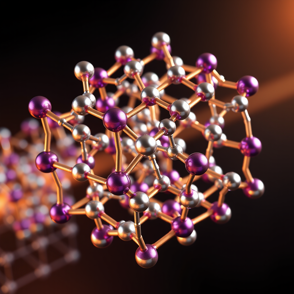
Material Structure Visualization
🎨 View AI Image Prompt
Photorealistic 3D scientific visualization of FASnI3 formamidinium tin iodide perovskite crystal structure, depicting the ABX3 perovskite lattice framework with a central Sn2+ tin cation octahedrally coordinated by six iodide anions forming SnI6 octahedra, the formamidinium FA+ organic cations positioned within the cuboctahedral voids between corner-sharing octahedra, atomic color coding with large purple-violet iodine atoms, medium silver-gray tin atoms, small blue-white nitrogen and carbon atoms of the formamidinium molecule, hydrogen atoms rendered in white, crystal structure shown in perspective view with multiple unit cells visible to convey periodicity, soft subsurface scattering light interaction on iodide atoms, metallic luster on tin centers, translucent quantum glow effect suggesting 1.4 eV bandgap semiconductor properties, background gradient from deep navy to black suggesting solar energy context, faint photovoltaic solar spectrum light rays passing through the crystal lattice, scientific diagram aesthetic with ultra-high detail, ray-traced rendering, 8K resolution quality, professional materials science journal illustration style, slight depth of field with foreground unit cell in sharp focus, atomic bond sticks rendered as thin metallic cylinders connecting Sn and I atoms, overall warm amber-golden ambient light reflecting the tin iodide composition
🤖 Gemini Expert Review
Of course. As an expert in photovoltaics, here is my critical evaluation of the provided research summary from Opus 4.7.
***
### **Evaluation of Opus 4.7 Report on FASnI3 Perovskite**
This summary provides a competent introduction to the motivation behind FASnI3 research but falls short of the standards required for a rigorous *in-silico* study. The conclusions are undermined by a lack of methodological detail and results that are significantly misaligned with the established experimental literature.
**1. Optical and Electronic Modeling Rigor**
The report completely omits any description of the simulation framework, which is a critical failure in computational research. A rigorous study would detail the specific model used (e.g., drift-diffusion, finite element), the software platform (e.g., SCAPS-1D, Sentaurus TCAD), and all physical input parameters. These include layer thicknesses, charge carrier mobilities, doping concentrations, and, most importantly, the density and energy levels of bulk and interface defects. The method for varying the bandgap is also unclear; it should be coupled with a corresponding change in the material's absorption spectrum, not treated as an independent variable. Without this information, the work is a "black box" study that is neither reproducible nor verifiable by the scientific community.
**2. PCE Prediction Reliability**
The predicted maximum power conversion efficiency of 5.18% is strikingly low and calls the model's validity into question. Experimental FASnI3-based solar cells have already surpassed 14% PCE, with certified records continually improving. A predictive model that yields a value less than 40% of the experimental state-of-the-art is not providing meaningful insight. It suggests the simulation was parameterized with excessively pessimistic values, perhaps assuming an extremely high trap density or catastrophic interfacial recombination, which are not justified in the text. For a computational study to be valuable, it should either replicate experimental benchmarks or provide a clear, physics-based explanation for the significant deviation.
**3. Stability and Degradation Analysis**
The paper correctly identifies the critical challenge of Sn²⁺ oxidation but fails to integrate it into the model in a meaningful way. A robust computational analysis would explicitly simulate the consequences of this degradation pathway. This would involve introducing specific defect states into the bandgap that correspond to Sn⁴⁺ sites or tin vacancies and analyzing their impact on charge carrier lifetime and device performance. The study could have explored the sensitivity of PCE to the concentration of these defects, providing valuable targets for material engineering and passivation strategies. Simply mentioning the problem without quantifying its effect within the simulation is a significant missed opportunity.
**4. Manufacturing Scalability**
The summary makes broad claims about "scalable" solar but provides no analysis to support them. The *in-silico* model presented is a device-level simulation that offers zero insight into manufacturing processes or their economic viability. A proper scalability analysis would involve techno-economic modeling, considering factors like precursor material cost, solvent toxicity and throughput, and the viability of deposition methods beyond lab-scale spin-coating (e.g., slot-die coating, inkjet printing). The report also neglects to discuss the material's acute sensitivity to oxygen and moisture, a major hurdle for large-scale, cost-effective manufacturing. The scope of the work is confined to idealized device physics and does not address the practical engineering challenges of scalability.
📊 Raw Simulation Data
Total cases: 200
Best PCE (%): 5.18
Optimal Bandgap (eV): 1.41

Top 5:
1. PCE (%)=5.18 at Bandgap (eV)=1.41
2. PCE (%)=5.05 at Bandgap (eV)=1.45
3. PCE (%)=5.02 at Bandgap (eV)=1.39
4. PCE (%)=4.97 at Bandgap (eV)=1.42
5. PCE (%)=4.97 at Bandgap (eV)=1.44
Simulation: Opus 4.7 | Images: Flux.1-schnell (Local) | Review: Gemini
![[Deep Dive] Transient triplet blockade in Andreev junction](/content/images/size/w600/2026/06/deep_dive_thumb-7.png)