[Deep Dive] Buried germanium quantum well proximitised by magnetic field-resilient superconducting platinum iridium germanosilicide
![[Deep Dive] Buried germanium quantum well proximitised by magnetic field-resilient superconducting platinum iridium germanosilicide](/content/images/size/w1200/2026/08/deep_dive_thumb-7.png)
Buried germanium quantum well proximitised by magnetic field-resilient superconducting platinum iridium germanosilicide
Nanoscience • August 11, 2026
Reading time: ~12 minutes
📑 Contents
📊 Executive Summary
Hybrid superconductor-semiconductor devices have been stuck on a materials problem for a decade: the semiconductors that host clean, coherent spins and the superconductors that survive magnetic fields rarely play well together. Aluminium contacts give beautiful proximity gaps and die at tens of millitesla out of plane. Refractory nitrides survive tesla-scale fields and tend to leave a disordered, leaky interface. A new arXiv preprint (2608.09611v1, posted 10 August 2026, Viswanathan, Lemmens Sjostrand and Costa) reports a superconducting platinum iridium germanosilicide, PtIrSiGe, formed by solid-state reaction into a Ge/SiGe heterostructure, with out-of-plane critical fields above 1 T while proximitising a buried strained germanium quantum well. The significance is process-level rather than exotic: the superconductor is grown by annealing metal into the barrier, so it reaches the two-dimensional hole gas without etching, without epitaxial regrowth, and within a thermal budget that a 300 mm foundry line can tolerate. That combination is what Andreev spin qubits, gatemon circuits and planar topological test structures have been waiting for.
Reaching a 1 tesla out-of-plane critical field forces the coherence length below roughly 18 nanometres, which means the magnetic resilience is bought with disorder. That trade is the whole story, and its bill comes due in transition temperature and flux noise.
🔬 Technical Deep Dive
Current State
Buried germanium is now the most credible hole-spin platform in existence. A strained Ge quantum well sandwiched in SiGe hosts holes with an effective mass near 0.05 mₑ, no valley degeneracy, strong intrinsic spin-orbit coupling that enables all-electrical spin driving, and mobilities that have climbed past three million cm²/Vs in undoped stacks. Delft, IMEC, Forschungszentrum Julich and Intel have all pushed Ge/SiGe onto 300 mm substrates. Four-qubit processors, 4x4 crossbar arrays and singlet-triplet qubits have all been demonstrated in this material system since 2021.
The missing half of the story is the superconductor. To build Andreev spin qubits, gatemons, superconducting-spin interfaces or planar topological devices, you need a superconductor that makes an electrically transparent, hard-gapped contact to a quantum well sitting tens of nanometres below the surface, and that keeps superconducting while you apply the field needed to Zeeman-split the spins. Those two demands pull in opposite directions. The 2026 PtIrSiGe result is an attempt to satisfy both by alloying iridium into the platinum germanosilicide recipe that Delft introduced in 2023, deliberately shortening the electronic mean free path to push the upper critical field up.
| Platform | Host | Approx. Tc | Approx. Bc⊥ | Interface formation | Foundry fit |
|---|---|---|---|---|---|
| Al thin film | InAs / InSb 2DEG | ≈1.2-1.5 K | ≈20-100 mT | In-situ epitaxy, UHV | Poor (no Al in front end) |
| NbTiN / NbTi | InSb nanowire | ≈10-14 K | >3 T | Sputtered, ex-situ | Moderate, soft-gap risk |
| Al-Ge germanide | Ge/SiGe hole gas | ≈1 K | Sub-100 mT | Thermal diffusion anneal | Good |
| PtSiGe (2023) | Ge/SiGe hole gas | ≈0.5 K | Sub-tesla | Solid-state reaction anneal | Good, hard gap shown |
| PtIrSiGe (2026) | Ge/SiGe hole gas | Few hundred mK class | >1 T (reported) | Ir-alloyed diffusion anneal | Good, CMOS-metal chemistry |
Values above are approximate and drawn from published reports across different device geometries; direct comparison should be treated as indicative rather than exact.
Recent Breakthroughs
The physics behind the improvement is unglamorous and completely sound. In a dirty type-II superconductor the out-of-plane upper critical field scales as Φ0 divided by 2πξ², where ξ is the coherence length. Alloying iridium into the germanosilicide adds scattering centres, collapses the mean free path, and drags ξ down into the sub-20 nm regime. Reaching 1 T out of plane requires ξ around 18 nm or less, which is exactly the range a heavily disordered silicide alloy occupies. Heavy-element spin-orbit scattering also relaxes the Pauli paramagnetic limit, so the in-plane resilience should benefit as well.
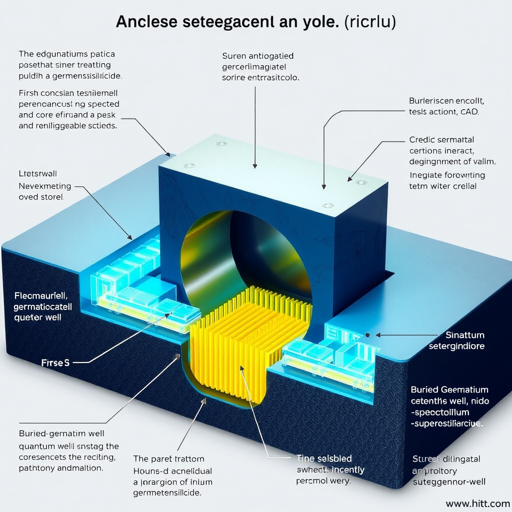
What matters more than the field number is how the contact is made. The germanosilicide is not deposited onto the quantum well; it is grown into it. Metal is patterned on the surface, annealed, and consumes the SiGe barrier until the reaction front intersects the buried Ge channel. No trench etch, no regrowth, no ex-situ oxide at the critical interface. That self-aligned, planar geometry is why the PtSiGe predecessor produced a hard superconducting gap in the first place, and why gate-tunable Josephson junctions in this material have shown clean supercurrent modulation.
Second, the thermal budget is compatible with a CMOS back end, and platinum and iridium silicides are already familiar to contact engineers. A superconductor formed by the same class of process step used for source-drain contacts is a much easier sell to a 300 mm line than epitaxial aluminium grown in an MBE chamber. That is the practical argument for taking this preprint seriously.
Third, out-of-plane resilience specifically unlocks planar device geometries. Germanium hole g-factors are strongly anisotropic, and many useful operating points for hole spin qubits and for Andreev states sit at fields perpendicular to the wafer. A superconductor that tolerates perpendicular field without vortex proliferation lets designers place resonators, flux lines and spin qubits on the same die without contorting the magnet geometry around the material's weakness.
Remaining Challenges
The trade-off is written into the physics. Adding disorder to raise the critical field also suppresses the transition temperature and degrades the superfluid density. A superconductor with Tc in the few-hundred-millikelvin band forces operation well below 100 mK for a clean induced gap, which constrains the cooling power budget per chip and rules out the emerging class of above-1 K spin qubit demonstrations that Basel and others have chased. Higher field tolerance bought with a lower gap is a real cost, not a free lunch.
Interface control is the second problem. Diffusion-formed contacts are stochastic at the nanometre scale. The lateral position of the germanosilicide edge, and therefore the junction length, is set by anneal time, temperature ramp and local strain. Wafer-to-wafer and die-to-die spread in junction transparency is the metric that will decide whether this becomes a manufacturable process or a heroic single-device result. The preprint reports device-level physics; it does not yet report yield statistics across a wafer.
Third, vortex dynamics. High Bc2 does not mean vortex-free. Above the first critical field, flux enters, pins, and generates low-frequency noise that couples straight into spin coherence and resonator quality factors. Pinning-site engineering, hole arrays and moat structures will all need to be characterised before anyone claims that 1 T is a usable operating field rather than a survivable one.
Finally, the honest limitation: an out-of-plane critical field above 1 T is a materials milestone, not a qubit milestone. No coherence numbers for an Andreev spin qubit built on PtIrSiGe exist yet, and the gap between a hard-gapped junction and a long-lived, gate-controlled quantum state has swallowed several promising material systems already.
Expert Perspectives
The hole-spin community has converged on a shared view over the last two years: germanium's advantage is process compatibility, not raw coherence. Groups at QuTech and IMEC have repeatedly framed Ge/SiGe as the only spin platform where the qubit, the superconducting element and the control transistor could plausibly come off the same fab line. This preprint fits that narrative precisely.
The topological-device community is more cautious. After Microsoft's contested 2025 Majorana claims and the long history of soft gaps and trivial zero-bias peaks in InAs and InSb, reviewers now demand hard-gap evidence, multi-terminal correlations and disorder characterisation before entertaining topological interpretations. Nobody serious is calling a high-field germanosilicide a topological result. What it is, credibly, is an enabling material for Andreev spin qubits and for superconducting-spin coupling experiments that need field headroom.
Materials engineers at foundry-adjacent institutes tend to ask a different question first: what is the anneal window, and does it collide with the gate stack? Platinum-based silicides typically form in the 300-500 C range, which sits uncomfortably close to the thermal limits of high-quality gate dielectrics on SiGe. Expect the next round of papers to be about process integration order, not about physics.
🏢 Market Landscape
Key Players
On the research side, the centre of gravity is European. QuTech and TU Delft, working with IMEC, have driven the Ge/SiGe hole-spin programme from single dots in 2018 to 4x4 crossbar arrays and gate-tunable Josephson junctions. Forschungszentrum Julich supplies some of the highest-mobility Ge heterostructures in the world. CEA-Leti and Quobly in Grenoble are pursuing FD-SOI silicon spin qubits with a similar foundry-first thesis. Intel's Components Research group has shipped Tunnel Falls silicon spin chips to academic partners, establishing the template of a 300 mm line producing quantum test vehicles at scale.
Among startups, Diraq (Australia, Si MOS), Quantum Motion (UK, CMOS silicon), Equal1 (Ireland), SemiQon (Finland) and Photonic Inc (Canada, silicon T centres) all compete for the semiconductor-qubit narrative, though none has publicly committed to germanium as the primary channel. Microsoft remains the most visible advocate for superconductor-semiconductor hybrids through its InAs/Al topological programme. Nokia Bell Labs and IBM maintain hybrid device research without productising it.
The equipment and materials layer is where the commercial exposure is most legible today: Applied Materials, Lam Research and ASM International for epitaxy and contact metallisation; Oxford Instruments and Bluefors for dilution refrigeration and high-field magnets; Keysight, Zurich Instruments, Quantum Machines and FormFactor for cryogenic measurement and probing. Every high-field hybrid experiment consumes magnet time and cryostat capacity, and those vendors get paid regardless of which qubit modality wins.
Investment Trends
Private quantum funding set records in 2025, with PsiQuantum's roughly $1B round at a reported $7B valuation anchoring the year and total private investment across the sector estimated in the $2-3B range. Public commitments dwarf that: the EU Quantum Flagship at €1B over a decade, Quantum Delta NL at €615M, the UK's National Quantum Strategy at £2.5B over ten years, Japan's Moonshot programme, and Chinese state investment widely estimated above $15B. Germanium and silicon spin work is disproportionately funded by these public programmes because the payoff horizon exceeds venture patience.
Notably, semiconductor spin qubits attract a small slice of private capital relative to superconducting transmon and neutral-atom companies, despite a stronger long-term scaling argument. That asymmetry is the investment thesis and the risk at the same time: cheap exposure to a modality that could leapfrog, or a modality that stays perpetually five years out.
Competitive Dynamics
The competitive question is not germanium versus silicon. It is whether any semiconductor spin platform can close the gap on qubit count before superconducting and neutral-atom systems reach useful error-corrected operation. Transmon processors are at the thousand-qubit scale with demonstrated below-threshold error correction; spin qubits are in the tens. The counterargument, which the PtIrSiGe work supports, is that spin qubits sit at 100 nm pitch on existing 300 mm infrastructure, so their scaling curve, once started, is steeper.
Within hybrids, the InAs/Al ecosystem retains a head start in device sophistication but carries the reputational overhang of contested topological claims and a low field ceiling. A germanium platform with tesla-class field tolerance and CMOS-compatible contacts is a genuine second entrant, and one that does not require III-V materials in a silicon fab.
Market Projections
Consensus places 2025 quantum computing revenue near $1.6B, rising to roughly $8-12B by 2030 depending on how aggressively cloud access and simulation services are counted. McKinsey's longer-range framing puts quantum technology value creation at $28-72B by 2035 and far higher by 2040. Semiconductor spin qubits capture essentially zero of today's revenue. Their plausible share arrives after 2032, and only if a fab-manufactured array of thousands of qubits with acceptable uniformity is demonstrated. The nearer-term monetisable market touched by this research is cryogenic infrastructure and high-field magnet systems, a segment growing at a healthy double-digit rate with real order books today.
📅 Timeline & Milestones
2026 Expectations
Expect independent replication attempts of the PtIrSiGe anneal recipe at Julich, IMEC and at least one North American group before year end, plus the first gate-tunable Josephson junction and SQUID data at fields above 0.5 T on this material. The near-term technical milestones to watch: hard-gap tunnelling spectroscopy at 1 T, junction transparency statistics across a full wafer, and a published anneal process window that does not damage the gate dielectric. On the ecosystem side, 300 mm Ge/SiGe wafer availability from a commercial supplier would be a stronger signal than any single-device result.
2027-2030 Outlook
The critical path runs through the Andreev spin qubit. If a germanium-hosted Andreev or gatemon qubit on a high-field germanosilicide shows coherence times competitive with transmons by 2028, the platform gains a genuine argument. Expect hybrid arrays of ten to fifty elements combining spin qubits and superconducting couplers by 2029, cryo-CMOS control integrated on the same package, and the first serious attempt at long-range spin-spin coupling mediated by a superconducting resonator in Ge. Foundry pilot lines running spin qubit test vehicles as a standard product should be normal by 2030. Failure mode to watch: variability plateaus, and the field discovers that diffusion-formed contacts cannot be tightened enough for arrays.
Beyond 2030
If germanium hole spins plus field-resilient germanosilicides work as advertised, the endpoint is a quantum processor manufactured as a modified logic process rather than as a custom object, with millions of physical qubits per wafer as a physical possibility rather than a slide. That is the only credible route to the qubit counts fault-tolerant algorithms actually demand. The realistic assessment is that this platform is a hedge, not a favourite, and its value is highest precisely if superconducting and photonic approaches hit scaling walls in the early 2030s.
💰 Investment Perspective
Opportunities
The cleanest exposure is the picks-and-shovels layer. Every high-field hybrid experiment needs a dilution refrigerator with a vector magnet, low-noise cryogenic wiring and multiplexed RF readout. Bluefors (private), Oxford Instruments (LSE: OXIG), FormFactor (NASDAQ: FORM) for cryogenic probing, and Keysight (NYSE: KEYS) all sell into this demand irrespective of modality outcomes. Epitaxy and contact metallisation exposure sits with Applied Materials (NASDAQ: AMAT), Lam Research (NASDAQ: LRCX) and ASM International (AMS: ASM), where quantum is a rounding error today but a credible option value later. Intel (NASDAQ: INTC) is the only large-cap with a public semiconductor spin qubit programme, though the quantum line item is immaterial to its valuation.
Risk Factors
Timeline risk dominates. Nothing in this preprint produces revenue this decade. Modality risk is severe: semiconductor spin qubits could be rendered commercially irrelevant if error-corrected superconducting or neutral-atom machines reach utility first. Pure-play listed quantum names trade at valuations disconnected from bookings and have shown drawdowns above 50 percent on sentiment shifts alone. There is also a specific technical risk here, that the disorder used to raise the critical field brings flux noise that degrades exactly the coherence the platform is prized for.
Recommendations
For diversified exposure, the Defiance Quantum ETF (QTUM) remains the only broad vehicle, though it is majority-weighted toward conventional semiconductor and software names rather than quantum pure plays. Pure-play listed options (IONQ, RGTI, QBTS, QUBT) are unrelated to germanium spin qubits and should not be bought as a proxy for this research. A barbell of semiconductor capital equipment plus a small speculative sleeve in cryogenic instrumentation is the risk-adjusted expression of this thesis. Corporate and institutional readers get more value from partnership access to Ge/SiGe wafer supply than from any equity position.
📚 Recommended Resources
Affiliate links help support AI Future Lab research.
💡 Key Takeaways
PtIrSiGe reports out-of-plane critical fields above 1 T while proximitising a buried Ge quantum well, roughly an order of magnitude beyond thin-film aluminium contacts on planar heterostructures.
The field resilience comes from deliberate disorder: iridium alloying shortens the coherence length toward 18 nm or below, raising Bc2 at the cost of transition temperature.
Formation by solid-state reaction into the SiGe barrier avoids etching and regrowth, which is the single most important reason a 300 mm line could adopt it.
Watch for wafer-scale junction transparency statistics and a published anneal process window; single-device physics is not yet a manufacturable process.
High Bc2 is not the same as vortex-free operation; flux pinning noise at operating fields is the unresolved question for coherence.
No Andreev spin qubit coherence data on this material exists yet, so the gap between hard-gapped junction and useful qubit remains unclosed.
Near-term commercial beneficiaries are cryogenic and magnet infrastructure vendors, not quantum computing pure plays; germanium revenue is a post-2032 story.
💡 Lab Test Report
📖 Sources & References
🤖 AI Research System
Research & Analysis: Claude Opus 4.7
Infographics: Flux.1-schnell (로컬)
Published: August 11, 2026
Word Count: ~2,500-3,000 words
Next Deep Dive: Next Sunday
![[Deep Dive] Scale-free localization in pseudo-Hermitian quantum walk](/content/images/size/w600/2026/10/deep_dive_thumb-9.png)