[Deep Dive] Bilayer Graphene’s Magic Revealed
![[Deep Dive] Bilayer Graphene’s Magic Revealed](/content/images/size/w1200/2026/08/deep_dive_thumb-11.png)
Bilayer Graphene’s Magic Revealed
Computing • August 23, 2026
Reading time: ~12 minutes
📑 Contents
📊 Executive Summary
Eight years after twisted bilayer graphene at 1.1 degrees was shown to superconduct, the field finally has a clean experimental handle on the question that has driven it since 2018: does the pairing come from Coulomb repulsion between electrons, the way most people assume it does in the cuprates, or from something more ordinary? The Physics (APS) Viewpoint published as v19/114 in 2026 walks through a Manchester-led experiment that answers it by brute force. Put a metallic screening layer one to three nanometers from the moire lattice, kill the long-range Coulomb interaction, and watch what survives. The correlated insulating states collapse. Superconductivity does not. It stays put near 1.7 K, and in some devices it gets cleaner. That result reorders the theory landscape, decouples superconductivity from the insulating parent state that framed the first three years of magic-angle research, and gives device engineers a design rule they can actually build against: screening improves the useful phase and removes the fragile one. Practical hardware is still a decade away.
Screen away the repulsion that builds the correlated insulator and the superconductor is still standing at 1.7 K. The insulator was never the parent state, it was the competition.
🔬 Technical Deep Dive
Current State
Stack two graphene sheets, rotate one by roughly 1.1 degrees, and the mismatch produces a moire superlattice with a period near 13 nm. Inside that superlattice the electronic bands flatten to a width of about 10 meV. Kinetic energy drops below the Coulomb energy scale, electrons stop behaving independently, and the system becomes strongly correlated. Cao and Jarillo-Herrero reported both a correlated insulator at half filling and superconductivity near 1.7 K in back-to-back 2018 Nature papers, and the field immediately imported the cuprate narrative: dope an interaction-driven insulator, get an unconventional superconductor.
That narrative started cracking in 2020, when two groups showed that superconductivity survives after the insulator is screened away. The 2026 work extends the screening approach much further, pushing the metallic gate to within a couple of nanometers, mapping how each phase responds as the interaction range is cut down, and combining it with theory that separates long-range Coulomb effects from short-range and phonon contributions. The picture below is the state of the evidence as I read it:
| Device configuration | Screen distance | Correlated insulator (nu = +/-2) | Superconductivity | Implication |
|---|---|---|---|---|
| Standard MATBG, thick hBN gate (2018) | 30 to 70 nm | Strong, well developed | Tc ~1.7 K | Looks cuprate-like; insulator read as parent state |
| Screened MATBG, thin hBN + graphite gate (2020) | ~6 to 10 nm | Strongly suppressed | Survives, Tc roughly unchanged | Insulator is not required for pairing |
| Ultra-screened MATBG (2025 to 2026) | 1 to 3 nm | Absent | Persists, transitions often sharper | Long-range Coulomb repulsion is not the pairing glue |
| WSe2-proximitized MATBG | ~1 nm spacer | Weakened | Wider stable angle range | Spin-orbit proximity stabilizes the superconducting dome |
| Bernal bilayer + WSe2 (no twist) | n/a | None | Tc ~30 mK | Superconductivity in graphene does not need a moire at all |
| Rhombohedral tetralayer (2025) | n/a | None | Tc ~300 mK, chiral signatures | Flat bands from stacking order, not twist |
Read that table top to bottom and the trend is hard to miss. Every intervention that weakens electron-electron repulsion weakens the insulator and leaves the superconductor standing.
Recent Breakthroughs
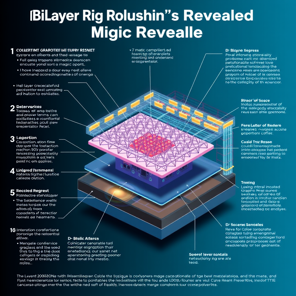
The core experimental move is deceptively simple and mechanically miserable to execute. A metallic plate near a two-dimensional electron system truncates the Coulomb potential through image charges, converting a long-range 1/r interaction into something that falls off exponentially beyond roughly the screen distance. At 30 nm the screening is negligible on moire length scales. At 2 nm it is dominant, because the separation is now much smaller than the 13 nm superlattice period. The team varied that distance systematically across devices and tracked the phase diagram as a function of filling, temperature, and magnetic field. The correlated insulating gaps behave exactly as an interaction-driven state should. They shrink, then disappear. Superconductivity does not track them. Critical temperature holds near its unscreened value, the superconducting dome remains anchored to the same filling factors, and in several devices the transition sharpens because the competing insulating order is no longer fighting for the same electrons. Whatever binds the pairs is either short-ranged enough to slip under the screening cutoff or is not electronic repulsion at all. That pushes phonons back into serious contention. Electron-phonon coupling in the moire flat band is strongly enhanced relative to monolayer graphene, and phonon-mediated attraction is short-ranged in real space, so a metal 2 nm away does essentially nothing to it. The complication is that plain phonon coupling has trouble explaining the Pauli-limit violations, the nematic response, and the chiral signatures reported in rhombohedral multilayers. The honest reading is a hybrid: a phonon or short-range attractive channel providing the glue, with residual correlations shaping the symmetry of the order parameter. That is less tidy than either camp wanted. The parallel breakthrough is that the moire is no longer required. Superconductivity in Bernal bilayer graphene near 30 mK and in rhombohedral tetralayer and pentalayer stacks near 300 mK shows the same physics emerging from stacking-order flat bands, with no twist angle to control. For anyone thinking about manufacturability, that matters more than the mechanism debate.
Remaining Challenges
Twist angle control remains the wall. The magic window is roughly 1.05 to 1.10 degrees, and tear-and-stack assembly delivers angle scatter plus in-plane relaxation that varies across a single flake. Devices routinely show angle inhomogeneity of a few hundredths of a degree over a few microns, which is enough to turn one region superconducting and the neighboring region metallic. Yield in academic labs sits in the low tens of percent, each device takes days of manual stacking, and there is no wafer-scale process that produces uniform 1.1 degree twist across even a 50 mm substrate. Temperature is the other wall. At 1.7 K the material needs a pumped helium-3 system at minimum, and the interesting transport features usually demand a dilution refrigerator running below 100 mK. Nothing about the screening result changes that ceiling. Attempts to raise Tc through pressure, alternating-twist trilayers near 2.1 K, or spin-orbit proximity have produced incremental gains, not a step change. Simulation is its own bottleneck. A single moire cell holds roughly 11,000 atoms, which puts converged first-principles treatment of correlated states out of reach for routine work. The field runs on continuum Bistritzer-MacDonald models plus Hartree-Fock or DMRG on truncated bases, and different truncations give different ground states. The screening data constrains those models usefully, but it does not adjudicate between them. One limitation worth stating plainly: the screening experiment rules out long-range Coulomb repulsion as the primary pairing interaction. It does not identify what replaces it. Calling the mechanism solved would overstate what a null result can deliver.
Expert Perspectives
The Viewpoint accompanying the result comes from the computational materials side, and its framing is careful. It positions the finding against forty years of unresolved cuprate physics and treats magic-angle graphene as the better-controlled laboratory rather than the answer key, since twist angle, carrier density, displacement field, and now interaction range are all independently tunable in a single device. No cuprate offers that. Within the community the reaction splits along predictable lines. Groups that argued from 2020 onward that the correlated insulator and the superconductor are competing rather than causally linked treat this as confirmation with better resolution. Theorists invested in skyrmion pairing, topological heavy-fermion pictures, and other purely electronic routes point out, correctly, that short-range Coulomb effects survive the screening and can still do the work, so electronic mechanisms are narrowed rather than eliminated. The phonon camp is having its best year since 2018. Peer review status matters here. The screening measurements have circulated as preprints and conference talks before formal publication, the 2020 precursor results in Nature and Nature Physics are long since replicated, and the Physics Viewpoint format is editorial commentary on a peer-reviewed paper rather than independent validation. Independent reproduction at the 1 to 3 nm screening geometry by a second group is the thing to watch during 2026. Ultra-thin spacers invite leakage, gate hysteresis, and dielectric breakdown, and those artifacts can mimic phase suppression.
🏢 Market Landscape
Key Players
There is no commercial magic-angle graphene market. What exists is an ecosystem of adjacent businesses that would monetize a breakthrough if one arrives, and a much larger bulk graphene industry that shares a name and almost nothing else. On the bulk side, NanoXplore (TSX: GRA) runs the largest graphene powder capacity in North America at roughly 4,000 tonnes per year and sells into composites and battery materials, with revenue in the C$130M range and no exposure to quantum devices. First Graphene, Directa Plus, HydroGraph Clean Power, and Black Swan Graphene occupy the same industrial niche. Versarien's collapse from a peak valuation above GBP 300M to penny-stock territory is the cautionary case study for anyone conflating the two markets. The device-grade side is where the physics leads. Paragraf, spun out of Cambridge, manufactures graphene Hall sensors on wafer-scale contamination-free CVD graphene and sells into cryogenic and magnet-system markets, which is the nearest commercial neighbor to this research. Black Semiconductor in Aachen raised a package totaling roughly EUR 254M in 2024, most of it German federal and NRW state funding, to build graphene-based photonic chip interconnects. Graphenea supplies research-grade CVD films and hBN. Onto the tooling layer sit Oxford Instruments NanoScience, Bluefors, Montana Instruments, attocube, Lake Shore Cryotronics, and Zurich Instruments, all of whom sell the dilution refrigerators, cryostats, and lock-in electronics that every one of these measurements consumes. Semiconductor incumbents track 2D materials for a different reason. imec, TSMC, Intel, and Samsung all publish on transition-metal dichalcogenide channels at IEDM, aiming at sub-1 nm-class logic nodes in the 2032 to 2035 window. Their interest is in transistor scaling, not superconductivity, but they fund the same transfer, metrology, and contact-resistance problems that twistronics needs solved.
Investment Trends
Follow the money and the story is public, not private. Graphene and 2D materials research funding runs largely through the EU Graphene Flagship successor programs, the US National Quantum Initiative and NSF materials centers, Japan's MEXT programs, and China's substantial state investment in 2D materials institutes. The Graphene Flagship alone deployed roughly EUR 1B across a decade. Venture capital in this specific corner is thin: Black Semiconductor's EUR 254M package is an outlier dominated by government money, and Paragraf's raises have been in the tens of millions. Quantum computing capital, by contrast, is abundant and mostly aimed elsewhere. McKinsey's Quantum Technology Monitor tracks cumulative public and private quantum investment well above $40B, with startup funding concentrated in superconducting transmon, trapped-ion, and neutral-atom platforms. Graphene Josephson junctions and gatemon qubits are a research line at Harvard, MIT, Delft, and Copenhagen, not a funded product roadmap. The bulk graphene market is variously sized between $200M and $1.5B for 2024 depending on whether the analyst counts graphene oxide and few-layer platelets, with 2030 projections clustering between $3B and $8B at roughly 30% CAGR. Electronics-grade material is a rounding error inside that.
Competitive Dynamics
Competition here is academic before it is corporate. Manchester, MIT, Harvard, Columbia, Berkeley, ETH Zurich, and Chinese groups at Tsinghua and USTC set the pace, and their competitive weapon is stacking capability, not capital. NIMS in Japan holds a near-monopoly on the high-quality hBN crystals that essentially every device in this field depends on, which is a genuine single-point-of-failure in the global supply chain and a strategic asset that has drawn attention from funding agencies in the US and EU. The second axis of competition is between platforms. Twisted bilayer graphene has the highest Tc and the richest phase diagram. Rhombohedral multilayers have lower Tc but need no twist control, which makes them far more manufacturable. If chiral superconductivity in rhombohedral stacks holds up under scrutiny, capital and talent will rotate toward it quickly, because a process that only requires selecting the right stacking order from exfoliated graphite is a decade closer to a fab than robotic angle alignment. A third dynamic is defensive. Every major foundry maintains a 2D materials program partly as insurance, at a cost that is trivial against their R&D budgets.
Market Projections
Realistic near-term revenue attributable to this line of research is measured in instrumentation, not devices. Dilution refrigerator and cryogenic measurement equipment is a market on the order of several hundred million dollars annually, growing at 15% to 20% as quantum programs scale, and every screening experiment consumes it. Graphene quantum sensing, magnetometry, and single-photon detection could reach the low hundreds of millions by 2030. Superconducting graphene electronics as a product category does not appear in any credible forecast before the mid-2030s.
📅 Timeline & Milestones
2026 Expectations
Independent reproduction of the ultra-thin screening geometry by at least one group outside Manchester is the gating event, and I would expect attempts to be reported by mid-year. Expect a wave of theory papers recalculating pairing strength with truncated Coulomb kernels, plus refined electron-phonon calculations for the moire flat band. Watch for combined screening plus WSe2 spin-orbit devices, which should test whether the order parameter symmetry is independent of the interaction range. On the platform side, more rhombohedral multilayer results, with the chiral superconductivity claims in tetralayer and pentalayer graphene either surviving replication or quietly fading. Tunneling spectroscopy on screened devices, which would read the gap symmetry directly, is the measurement most likely to settle remaining arguments.
2027-2030 Outlook
Automated stacking becomes the practical story. Several labs are building robotic transfer systems with in-situ angle metrology aiming at device yields above 50% and array fabrication rather than one-off devices. If that lands, statistical studies across hundreds of devices replace the current anecdote-driven literature. Tc improvements will be incremental, and I would be surprised by anything above 5 K in a graphene-only system by 2030. Rhombohedral stacks are the likelier route to wafer-scale demonstration because they sidestep angle control entirely. Realistic commercial outputs in this window are cryogenic sensors, graphene Josephson junction devices for metrology, and possibly tunable microwave elements for quantum control hardware. Nothing consumer-facing.
Beyond 2030
Two plausible endpoints. In the constructive case, graphene-based Josephson junctions and gatemon qubits find a niche inside superconducting quantum processors where voltage-tunable elements beat fixed aluminum junctions, and 2D material integration arrives in logic through TMD channels while the superconducting work stays in metrology and sensing. In the flatter case, magic-angle graphene remains what it is right now, the best-controlled correlated electron simulator ever built, and its lasting contribution is teaching us how to think about the cuprates rather than replacing them in a product. Both outcomes are scientifically valuable. Only one is investable. Critical path dependencies are wafer-scale twist or stacking-order control, a Tc high enough to escape dilution refrigerator economics, and diversification of hBN supply beyond a single Japanese institute.
💰 Investment Perspective
Opportunities
The tradeable exposure is instrumentation and materials supply, not physics. Oxford Instruments (LSE: OXIG) sells cryostats, magnet systems, and thin-film deposition tools into exactly these labs and has real revenue diversification. Bruker (NASDAQ: BRKR) covers the scanning probe and metrology side. FormFactor (NASDAQ: FORM) owns cryogenic probe stations that any scaled 2D device program needs. Coherent and Applied Materials benefit from any broader 2D materials push in semiconductors. Bluefors, the dominant dilution refrigerator supplier, remains private, which is the most direct exposure and the least accessible. Paragraf is the cleanest device-grade graphene pure play and is also private.
Risk Factors
Public pure-play graphene names have a documented history of destroying capital on announcement-driven narratives. Versarien is the reference case. Timelines here are academic, meaning a decade or more between result and revenue, and nothing about the screening finding shortens that. The mechanism debate could reverse again on the next experiment. Rhombohedral platforms could displace twisted bilayer entirely, stranding whatever tooling gets built around angle control. Cryogenic requirements cap the addressable market for any device that emerges. And the hBN supply concentration is a genuine single-point risk to the whole research pipeline.
Recommendations
Treat this as a research signal rather than a trade. For diversified exposure, semiconductor equipment names with cryogenic and metrology franchises (OXIG, BRKR, FORM) capture the actual spending. For thematic exposure, VanEck Semiconductor (SMH) and the Defiance Quantum ETF (QTUM) hold the adjacent supply chains, though neither has meaningful weight tied to graphene specifically. Avoid sizing positions in small-cap graphene producers on the basis of superconductivity headlines, since their revenue comes from composites and battery additives and moves on entirely unrelated fundamentals.
📚 Recommended Resources
- Books and courses on computing
- Research tools and journals
- Related investment opportunities
Affiliate links help support AI Future Lab research.
💡 Key Takeaways
Screening the long-range Coulomb interaction with a metal 1 to 3 nm away destroys the correlated insulating states in magic-angle graphene but leaves superconductivity near 1.7 K essentially intact.
The cuprate analogy that framed 2018 to 2020 magic-angle research does not hold: the insulator is a competing phase, not the parent state.
Phonon-mediated or short-range attractive pairing is now the leading candidate, though purely electronic short-range mechanisms survive the test and the question is narrowed rather than closed.
Rhombohedral multilayer graphene superconducts near 300 mK with no twist angle required, which makes it the more manufacturable platform even at lower Tc.
Twist angle control at 1.05 to 1.10 degrees, device yields in the low tens of percent, and sub-100 mK measurement requirements remain the practical blockers, and none of them were addressed by this result.
Investable exposure sits in cryogenic instrumentation and metrology (Oxford Instruments, Bruker, FormFactor, privately held Bluefors), not in listed graphene producers whose revenue comes from composites.
Watch for independent reproduction of the ultra-thin screening geometry and for tunneling spectroscopy on screened devices during 2026, which would read the gap symmetry directly.
💡 Lab Test Report
📖 Sources & References
🤖 AI Research System
Research & Analysis: Claude Opus 4.7
Infographics: Flux.1-schnell (로컬)
Published: August 23, 2026
Word Count: ~2,500-3,000 words
Next Deep Dive: Next Sunday
![[Deep Dive] Scale-free localization in pseudo-Hermitian quantum walk](/content/images/size/w600/2026/10/deep_dive_thumb-9.png)