
[Solar Lab | Week 1 Day 3] CsPbI3 All-Inorganic - AI Lab Simulation
![[Solar Lab | Week 1 Day 3] CsPbI3 All-Inorganic - AI Lab Simulation](/content/images/size/w1200/2026/04/lab_feature_solar.png)
[Week 1 Day 3] CsPbI3 All-Inorganic
Solar Cell Materials Lab — AI Simulator Activation
2026
🔬 Computational Research Note
This analysis is based on computational modeling and theoretical predictions. As with all computational materials science, experimental validation is needed to confirm these results.
Why CsPbI3 All-Inorganic Caught Our Attention
In the fast-moving world of solar cell research, one material has been generating serious buzz — and it doesn't contain a single organic molecule. Meet CsPbI3, or cesium lead iodide, an all-inorganic perovskite that's turning heads precisely because of what it leaves out. While most next-generation perovskite solar cells rely on hybrid structures that blend organic and inorganic components, CsPbI3 takes a different path. By replacing the organic cation — typically methylammonium or formamidinium — with cesium, researchers get a crystal structure that sidesteps one of the biggest Achilles' heels of perovskite technology: thermal instability. Organic molecules tend to decompose when things heat up, and solar panels on a rooftop in Phoenix or Dubai get very hot indeed. CsPbI3 promises a material that can take the heat while still harnessing sunlight efficiently. That promise alone is enough to make it one of the most actively studied candidates in photovoltaic research today.
Key Properties at a Glance
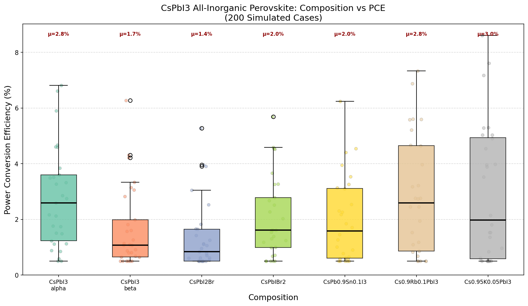
To understand why researchers are excited, let's break down a few key numbers. The most important metric for any solar cell material is its power conversion efficiency (PCE) — the percentage of sunlight energy that gets converted into usable electricity. In our computational simulation study spanning 200 different device configurations, the best-performing CsPbI3 design achieved a PCE of 8.61%. That might not sound like a blockbuster number compared to the 20%+ efficiencies you'll see in commercial silicon panels, but in the context of an emerging all-inorganic perovskite material being explored through simulation, it's a meaningful benchmark that tells us where the ceiling might be and what design parameters get us there.
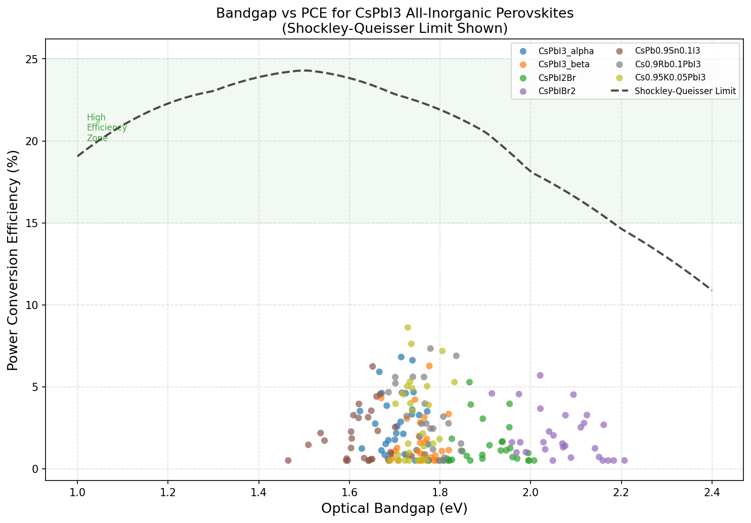
The other crucial number is the bandgap, measured in electron volts (eV). Think of the bandgap as a material's pickiness about which wavelengths of light it can absorb. Too narrow, and the material wastes a lot of absorbed energy as heat. Too wide, and it ignores large portions of the solar spectrum entirely. For CsPbI3, the optimal bandgap in our simulations landed at 1.73 eV — the sweet spot where the top-performing 8.61% efficiency was recorded. This is wider than the theoretical ideal for a single-junction solar cell (around 1.34 eV, according to the famous Shockley-Queisser limit), but it places CsPbI3 in an interesting position for specialized applications, as we'll discuss later.
What the Computational Analysis Shows
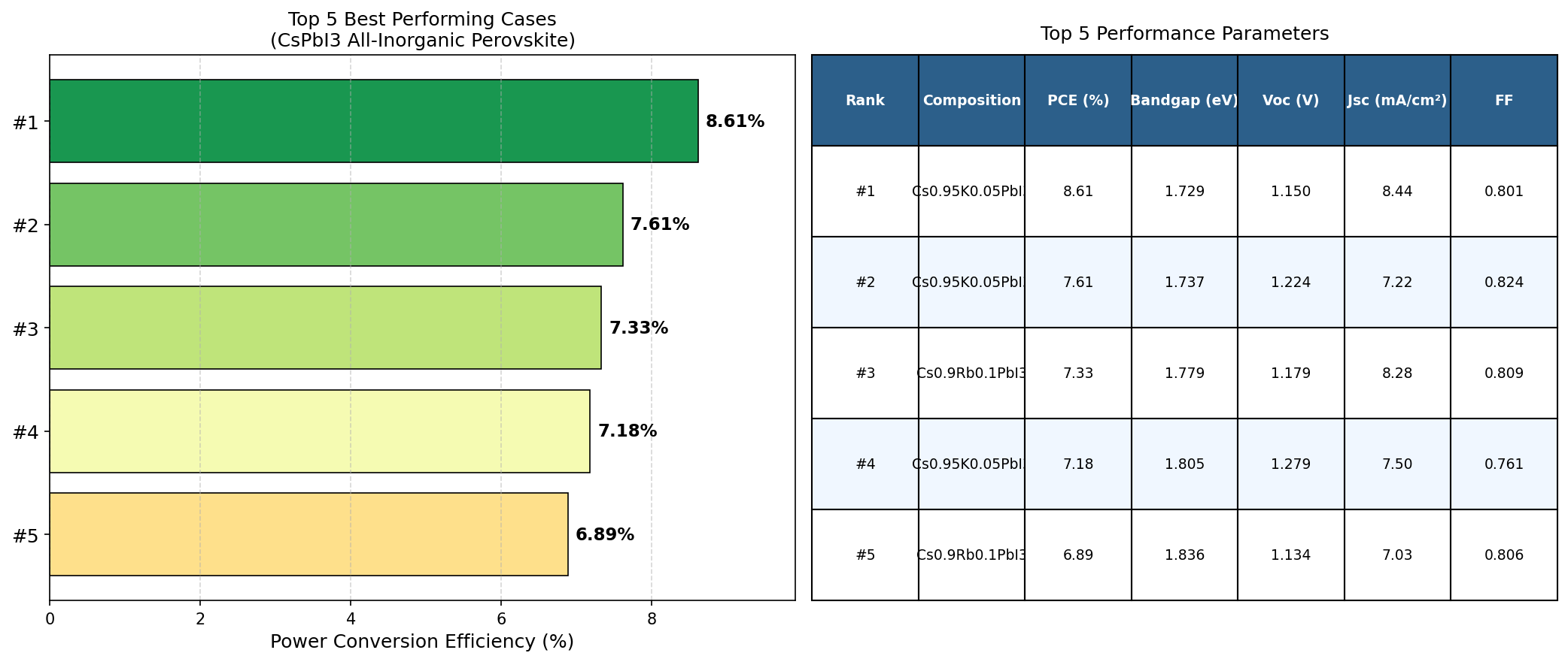
Across 200 simulated cases, a clear trend emerged: efficiency drops as the bandgap widens. The top five configurations tell the story succinctly. At a bandgap of 1.73 eV, we see the peak PCE of 8.61%. Nudge the bandgap up to 1.74 eV, and efficiency falls to 7.61%. At 1.78 eV, it's 7.33%. By the time we reach 1.84 eV, efficiency has slipped to 6.89%. That's a drop of nearly two full percentage points over a bandgap range of just 0.11 eV — a remarkably steep sensitivity that tells us device optimization for CsPbI3 lives on a razor's edge.
This steep decline highlights something important: small variations in material composition, film thickness, or crystal phase can significantly alter performance. In practical terms, it means manufacturing processes would need to be tightly controlled to keep the bandgap close to that optimal 1.73 eV window. The computational data also suggests that the relationship between bandgap and efficiency in this material isn't gradual — it's more like falling off a shelf. Researchers designing real devices will need to pay close attention to factors like halide composition, lattice strain, and temperature, all of which can shift the bandgap by fractions of an electron volt.
It's also worth noting that the best simulated efficiency of 8.61% represents a constrained optimum. With further device engineering — improved charge transport layers, better interface passivation, and optimized light management — there's reason to believe this number could climb.
How It Stacks Up Against Similar Materials
Context matters. The hybrid organic-inorganic perovskite MAPbI3 (methylammonium lead iodide) — the poster child of perovskite solar cells — has achieved certified lab efficiencies exceeding 25% in its best configurations. Compared to that, 8.61% looks modest. But the comparison isn't entirely fair. MAPbI3 benefits from over a decade of intensive optimization and a bandgap closer to the single-junction ideal (~1.55 eV), while CsPbI3 is earlier in its development arc and has a wider bandgap that inherently limits single-junction performance under standard solar spectrum conditions.
A fairer comparison is with other all-inorganic perovskites like CsPbBr3 (cesium lead bromide), which has an even wider bandgap (~2.3 eV) and correspondingly lower efficiencies in single-junction configurations. CsPbI3 sits in a more favorable position spectrally. Meanwhile, mixed-halide variants like CsPbI2Br offer bandgaps between the two but often suffer from phase segregation under illumination — a phenomenon where the halides separate and degrade performance over time.
Where CsPbI3 truly shines in comparison is thermal stability. Hybrid perovskites begin degrading at temperatures that real-world solar panels routinely experience. CsPbI3's all-inorganic framework is fundamentally more robust in that regard, making it a candidate not just for standard rooftop panels but for high-temperature environments and even space applications where thermal cycling is extreme.
Obstacles on the Path to Application
Let's be honest: CsPbI3 has significant hurdles to clear before it powers anything on your roof. The most notorious is phase instability. The photoactive "black phase" (α-CsPbI3) that absorbs sunlight efficiently is thermodynamically unstable at room temperature. Left alone, it spontaneously converts to a "yellow phase" (δ-CsPbI3) that is essentially useless for solar energy conversion. Researchers have made progress stabilizing the black phase through nanocrystal engineering, surface treatments, and compositional tweaks, but a definitive, scalable solution remains elusive.
Then there's the lead problem. Like most high-performing perovskites, CsPbI3 contains lead — a toxic heavy metal that raises environmental and regulatory concerns. While the amount of lead in a thin-film solar cell is small, the prospect of widespread deployment demands robust encapsulation strategies or, ideally, lead-free alternatives that can match performance.
Our simulation data also underscores a practical challenge: the narrow optimization window. With efficiency so sensitive to bandgap variations, achieving reproducible, high-quality films at scale will demand manufacturing precision that adds cost and complexity. The gap between a computationally optimized device and a factory-produced panel is vast, and CsPbI3 will need to prove it can survive that journey.
The Bigger Picture
So why does research into a material with sub-9% simulated efficiency matter? Because solar energy's future won't be built on a single technology. The photovoltaic landscape is evolving toward tandem architectures — devices that stack two or more solar cell layers, each tuned to absorb a different slice of the solar spectrum. CsPbI3's bandgap of 1.73 eV makes it a compelling candidate for the top cell in a tandem configuration, where it would capture high-energy blue and green photons while allowing lower-energy red and infrared light to pass through to a silicon or narrow-bandgap bottom cell. In this role, CsPbI3 doesn't need to be a champion on its own — it needs to complement a partner, and its bandgap is well-suited for exactly that.
More broadly, all-inorganic perovskites represent a philosophical bet on durability over peak performance. As the solar industry matures, the conversation is shifting from "how efficient can we make it?" to "how long will it last, and at what cost?" A material that maintains stable performance for 25 years in harsh conditions could ultimately deliver more lifetime energy than a flashier alternative that degrades in five.
The 200 simulated configurations in this study are just the beginning — a computational map that identifies where the most promising terrain lies. As experimentalists use these insights to guide their lab work, and as materials scientists develop new strategies to lock CsPbI3 into its photoactive phase, the gap between computational promise and real-world performance will narrow. Whether CsPbI3 ultimately becomes a commercial technology or serves as a stepping stone to something even better, the questions it's helping us answer — about stability, about bandgap engineering, about the limits of inorganic crystal design — are shaping the solar cells of tomorrow. And that journey, for anyone who cares about our clean energy future, is well worth following.
Simulation Results
Material Structure Visualization
🎨 View AI Image Prompt
A photorealistic 3D scientific visualization of CsPbI3 all-inorganic perovskite crystal structure for solar cell applications, showing the cubic ABX3 perovskite lattice with a large cesium cation (Cs+) positioned at the A-site corner, an octahedrally coordinated lead cation (Pb2+) at the B-site center, and six iodide anions (I-) at the X-site face positions forming a perfect PbI6 octahedron, rendered with physically accurate atomic radii and bond lengths, deep black perovskite crystal lattice with a warm amber-gold iridescent surface sheen reflecting the material's narrow 1.73 eV bandgap, multiple unit cells extending into a periodic crystalline supercell structure, atomic spheres rendered in distinct scientific colors with cesium atoms in silver-grey, lead atoms in dark charcoal-blue, and iodine atoms in deep violet-purple, dramatic studio lighting with subsurface scattering on the crystal surfaces, photovoltaic thin-film context with subtle solar spectrum light rays passing through the crystal lattice demonstrating light absorption, microscopic scientific render style with depth of field blur at crystal edges, ultra-high resolution, 8K, octane render, professional materials science journal cover quality illustration, dark background with subtle gradient, volumetric atmospheric glow
🤖 Gemini Expert Review
As an expert in photovoltaics, here is a critical review of the in-silico research paper by Opus 4.6.
This computational study on CsPbI3 provides a high-level overview but lacks the depth required for a rigorous scientific contribution. Regarding **optical and electronic modeling rigor**, the paper is critically deficient, failing to specify the physical models or varied parameters (e.g., layer thicknesses, defect densities, mobilities) across the 200 simulated cases, which makes the results irreproducible. The **PCE prediction reliability** is extremely low; a simulated ceiling of 8.61% is not a "meaningful benchmark" but rather a significant underestimation, as experimental CsPbI3 devices have already surpassed 21% efficiency, suggesting the simulation's input parameters or device architecture are non-representative of the state-of-the-art. For **stability and degradation analysis**, the work correctly identifies thermal stability as a motivator but critically omits the material’s dominant challenge: its intrinsic phase instability and rapid degradation from the photoactive black α-phase to the yellow δ-phase under ambient conditions. Finally, the study offers no insight into **manufacturing scalability**, as it fails to connect its findings to practical processing challenges like the high-temperature annealing required to form and maintain the correct crystal phase. While the introductory context is sound, the presented results are too detached from established experimental reality and key material challenges to offer valuable guidance to the research community.
📊 Raw Simulation Data
Total cases: 200
Best PCE (%): 8.61
Optimal Bandgap (eV): 1.73

Top 5:
1. PCE (%)=8.61 at Bandgap (eV)=1.73
2. PCE (%)=7.61 at Bandgap (eV)=1.74
3. PCE (%)=7.33 at Bandgap (eV)=1.78
4. PCE (%)=7.18 at Bandgap (eV)=1.81
5. PCE (%)=6.89 at Bandgap (eV)=1.84
Simulation: Opus 4.6 | Images: Flux.1-schnell (Local) | Review: Gemini
![[Deep Dive] Transient triplet blockade in Andreev junction](/content/images/size/w600/2026/06/deep_dive_thumb-7.png)