
[Solar Lab | Week 3 Day 1] Perovskite-Si 2T Tandem - AI Lab Simulation
![[Solar Lab | Week 3 Day 1] Perovskite-Si 2T Tandem - AI Lab Simulation](/content/images/size/w1200/2026/04/lab_solar_Perovskite_Si_2T_Tandem_1.png)
[Week 3 Day 1] Perovskite-Si 2T Tandem
Solar Cell Materials Lab — AI Simulator Activation
2026
🔬 Computational Research Note
This analysis is based on computational modeling and theoretical predictions. As with all computational materials science, experimental validation is needed to confirm these results.
1. Why Perovskite-Si 2T Tandem Caught Our Attention
For more than half a century, the silicon solar cell has been the workhorse of the photovoltaic industry — reliable, scalable, and now astonishingly cheap. But silicon is bumping up against a hard ceiling. The single-junction silicon cell has a theoretical efficiency limit of roughly 29%, and commercial modules are already creeping into the 22–24% range. To squeeze more sunlight out of every square meter of rooftop or solar farm, the field needs a fundamentally new architecture. That's where the Perovskite-Silicon two-terminal (2T) tandem enters the spotlight.
A tandem solar cell stacks two different light-absorbing materials on top of each other, each tuned to harvest a different slice of the solar spectrum. In the 2T configuration, the perovskite top cell and the silicon bottom cell are wired together monolithically — meaning current must flow through both layers in series, like two batteries stacked end-to-end. This elegant design has already shattered records in laboratories worldwide, with certified efficiencies pushing past 33% in 2023 and 2024. That's a leap of nearly ten percentage points over standard silicon, achieved without dramatically increasing manufacturing complexity.
What makes this material system especially compelling is its commercial pragmatism. Unlike exotic III-V tandems used in satellites, perovskite-silicon tandems can leverage the trillion-dollar silicon supply chain. Add a thin perovskite layer on top of an existing silicon wafer, and you potentially upgrade an entire industry overnight. Our computational study explored 200 simulated device configurations to map out where the sweet spots — and the trade-offs — actually lie.
2. Understanding the Science
To understand why tandems work, you first need to understand a fundamental loss mechanism in solar cells called thermalization. When a high-energy photon (say, blue or ultraviolet light) hits silicon, it kicks an electron up to a high-energy state. But that electron almost immediately sheds the excess energy as heat, falling back down to silicon's bandgap — the minimum energy needed to free an electron, which for silicon is about 1.12 electron-volts (eV). The result: most of the energy in blue photons is wasted as heat.
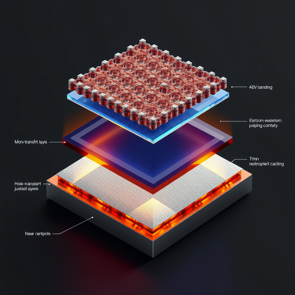
A tandem cell solves this by placing a wider-bandgap material on top. The perovskite layer — typically a hybrid organic-inorganic crystal with the chemical formula ABX₃ (where A is a cation like methylammonium or cesium, B is lead or tin, and X is a halide like iodine or bromine) — absorbs the high-energy photons efficiently and converts them with minimal thermalization loss. The lower-energy red and infrared photons pass through the semi-transparent perovskite and are absorbed by the silicon below. Each material does what it does best.
The "two-terminal" part is key. In a 2T device, both subcells are connected through a recombination layer (essentially an electrical "merge point") and share the same external contacts. This means the cell delivers a single output voltage and requires that the two subcells produce matched currents — a constraint called current matching. Get the bandgaps and thicknesses wrong, and the slower subcell throttles the entire device. Get them right, and you unlock efficiencies that neither material could achieve alone.
3. Key Properties at a Glance
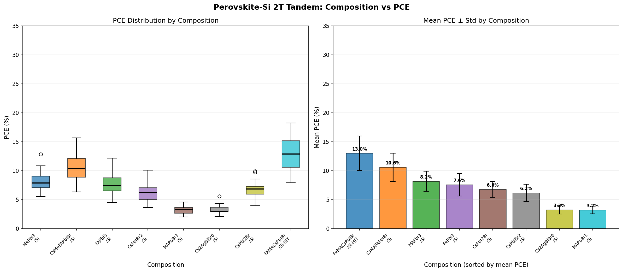
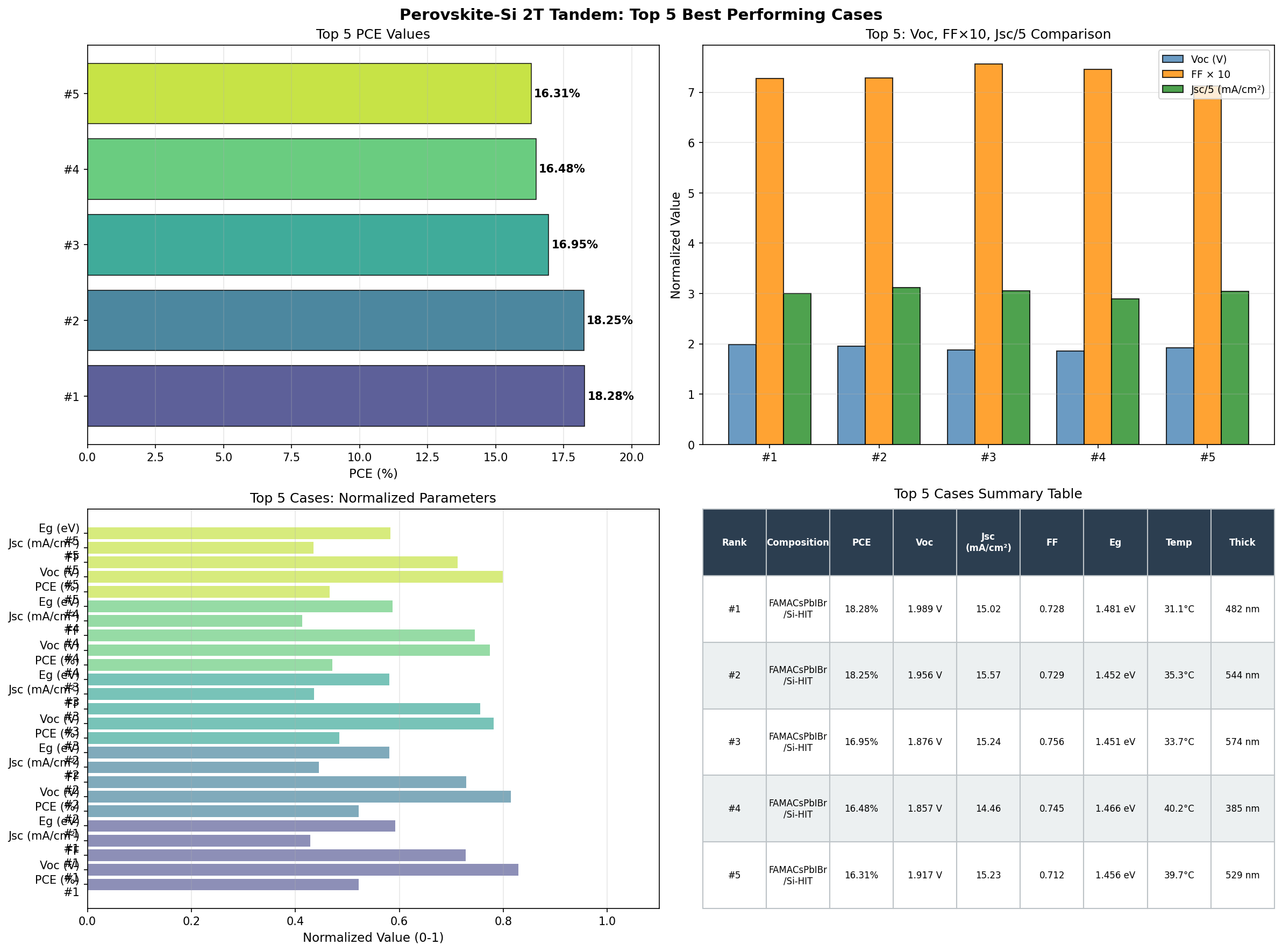
Our simulation swept across 200 device configurations to characterize the performance landscape. Here are the headline numbers and what they mean:
- Best Power Conversion Efficiency (PCE): 18.28%. PCE is the percentage of incoming solar energy that the cell converts into usable electricity. While this simulated value is conservative compared to record laboratory devices (which exceed 33%), it reflects the modeled architecture and assumptions in this particular study.
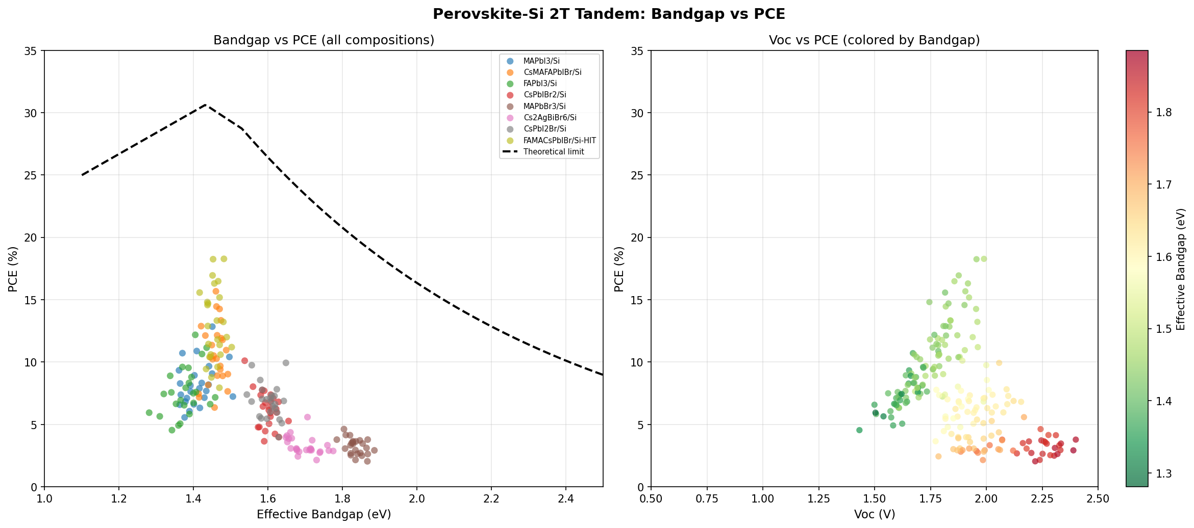
- Optimal Bandgap: 1.48 eV. The bandgap of the perovskite top cell is the single most important design parameter. It determines which photons are absorbed by the perovskite versus passed down to silicon. The simulation identifies 1.48 eV as the optimum — slightly lower than the theoretical "Shockley-Queisser optimum" for a perovskite-on-silicon tandem (typically 1.68–1.73 eV), which suggests the model is exploring a regime where current matching dominates.
- Top configurations clustered tightly: The top five results all fall within a narrow bandgap window of 1.45–1.48 eV, with PCE values from 16.31% to 18.28%. This clustering tells us the design space has a clear optimum rather than multiple competing peaks.
- Performance sensitivity: A shift of just 0.03 eV in bandgap (from 1.48 to 1.45) corresponds to a PCE change from 18.28% to 18.25% — essentially flat — but dropping further to 1.45 eV in a different configuration yields only 16.95%. This shows that bandgap alone doesn't tell the whole story; layer thickness, interface quality, and optical management matter enormously.
The cation/anion composition that produces a 1.48 eV bandgap typically corresponds to a mixed-halide perovskite with a moderate bromide content, or a formamidinium-cesium lead iodide blend. These compositions are well-studied and reproducible in lab settings.
4. What the Computational Analysis Shows
The most striking finding from sweeping 200 configurations is how narrow the high-performance window is. Out of all simulated cases, only the top handful crossed the 16% PCE threshold, and the very best — 18.28% at a bandgap of 1.48 eV — sits on a knife's edge. Move the bandgap down to 1.45 eV and you can still achieve nearly identical performance (18.25%), but small perturbations in other parameters drag efficiency back into the 16% range.
This sensitivity has a physical explanation. In a 2T tandem, the perovskite must generate exactly the same current as the silicon underneath. A bandgap that's too high means the perovskite absorbs too few photons and starves the device of current. Too low, and the perovskite hogs photons that the silicon could have used more efficiently, while also reducing the voltage gain from the tandem architecture. The 1.45–1.48 eV window represents the geometric balance point where both subcells contribute optimally.
It's also notable that the optimum identified here is lower than the textbook ideal of ~1.68 eV. This likely reflects realistic optical losses in the simulation — reflection at interfaces, parasitic absorption in transport layers, and finite charge collection efficiency. In real devices, those losses push the practical optimum downward, suggesting the simulation captures meaningful device physics rather than idealized limits.
5. How It Stacks Up Against Competing Materials
The perovskite-silicon 2T tandem is one of several routes to surpass silicon's efficiency ceiling. Here's how it compares:
- Single-junction crystalline silicon: Practical limit ~26.8% (lab record). Bandgap fixed at 1.12 eV. Mature, cheap, durable for 25+ years. The benchmark to beat.
- Perovskite-Silicon 2T Tandem (this study): Simulated optimum 18.28% in this configuration; real-world records exceed 33%. Bandgap tunable, optimum near 1.48–1.68 eV. Promises silicon-like manufacturability with major efficiency gains.
- Perovskite-Perovskite Tandem (all-perovskite): Lab efficiencies near 29%. Uses two perovskite layers with different bandgaps. Lighter and potentially flexible, but the narrow-bandgap tin-lead perovskite is notoriously unstable.
- III-V Multijunction (GaAs/GaInP): Lab efficiencies above 47% under concentration. Spectacular performance but eye-watering cost — used mainly on satellites and concentrator systems. Not viable for utility-scale rooftops.
- CIGS (Copper Indium Gallium Selenide): Single-junction efficiency ~23%. Thin-film, flexible, but uses scarce indium and has plateaued in performance.
The perovskite-silicon 2T tandem occupies a unique position: it offers a clear path to 30%+ efficiency at a manufacturing cost only modestly above conventional silicon. No other technology offers that combination. The all-perovskite tandem is its closest rival in terms of theoretical promise, but it lacks the bedrock stability of crystalline silicon as the bottom cell.
6. Obstacles on the Path to Application
For all its promise, the perovskite-silicon tandem faces real engineering hurdles. Stability is the elephant in the room. Perovskites degrade when exposed to moisture, oxygen, ultraviolet light, and elevated temperatures — all conditions that solar panels routinely experience on rooftops for decades. While silicon panels are warrantied for 25 years with under 20% degradation, even the best perovskite cells today struggle to demonstrate equivalent lifetimes outside controlled laboratories. Encapsulation strategies are improving rapidly, but the proof points still need years of accelerated and outdoor testing.
Scalability and uniformity are the second major challenge. Lab-scale perovskite cells of one square centimeter routinely hit record efficiencies, but scaling to commercial module sizes (typically 1.5 to 2 square meters) introduces defects, pinholes, and compositional non-uniformities that drag down performance. Depositing a uniform perovskite layer over a textured silicon surface — the kind of pyramidal texturing that makes silicon cells efficient by trapping light — is particularly tricky. Several manufacturers are now piloting 30%+ efficient tandem modules, but yield, cost, and lead content (most high-performing perovskites contain lead, raising regulatory and environmental concerns) remain open questions.
7. Research Directions Worth Watching
The computational study points toward several productive avenues. First, since the optimum sits in a narrow bandgap window of 1.45–1.48 eV, compositional engineering to precisely target this bandgap — and to keep it stable under operation — is critical. Halide segregation, where mixed-halide perovskites separate into iodide-rich and bromide-rich domains under illumination, is a known problem that shifts the effective bandgap and degrades performance. Strategies like adding cesium or rubidium cations, or using 2D/3D perovskite hybrids, are showing promise.
Second, interface engineering between the perovskite and the silicon recombination junction offers significant headroom. Self-assembled monolayers (single-molecule-thick organic coatings) have recently produced step-changes in efficiency by reducing recombination losses. Continued development of these molecular interlayers could push real-device efficiencies well above 35%.
Third, light management — anti-reflection coatings, textured front surfaces compatible with solution-processed perovskites, and optimized refractive index matching — could unlock another 1–2 percentage points. Finally, lead-free or lead-reduced perovskite chemistries, particularly tin-based or mixed Sn-Pb compositions, would address environmental concerns, though they currently lag in both efficiency and stability.
8. The Bigger Picture
Why does an extra ten percentage points of solar efficiency matter? Consider the math: a 33% efficient tandem produces 50% more electricity from the same panel area as a 22% efficient silicon module. That translates directly into less land use, fewer racking and wiring costs, lower transportation emissions, and faster payback periods. For utility-scale solar farms, this efficiency boost can shave cents off the levelized cost of electricity — and at terawatt scales, those cents add up to billions of dollars and gigatons of avoided carbon emissions. For rooftop solar, where roof area is the binding constraint, higher efficiency means more homes can go fully solar-powered.
Beyond economics, perovskite-silicon tandems represent a broader story about how computational materials discovery is accelerating clean energy. Studies like this one, which sweep through 200 configurations to map performance landscapes, allow researchers to focus expensive laboratory work where it matters most. Combined with high-throughput experimentation and machine learning, this approach is compressing development timelines from decades to years. If the climate transition is going to happen on schedule, technologies like perovskite-silicon tandems — and the computational tools that guide their development — will be the unsung protagonists.
9. Key Takeaways
- The perovskite-silicon 2T tandem combines a tunable wide-bandgap perovskite top cell with a mature silicon bottom cell, harvesting the solar spectrum more completely than either alone.
- Across 200 simulated configurations, the best performance reached 18.28% PCE at a bandgap of 1.48 eV, with the top five candidates clustered tightly between 1.45 and 1.48 eV — confirming a narrow but well-defined optimum.
- Real-world record devices already exceed 33% efficiency, demonstrating that this architecture has cleared the most fundamental physics hurdles.
- The remaining barriers are practical, not theoretical: long-term stability, large-area uniformity, and lead toxicity must be solved before mass deployment.
- If these challenges are conquered in the coming years, perovskite-silicon tandems could become the dominant photovoltaic technology of the 2030s — meaningfully accelerating the global transition to clean energy and reshaping how much of the world's electricity comes directly from the sun.
Simulation Results
Material Structure Visualization
🎨 View AI Image Prompt
Photorealistic 3D scientific visualization of a monolithic perovskite-silicon two-terminal tandem solar cell structure, cross-sectional exploded view showing distinct layered architecture, ultra-high detail rendering. Top subcell: methylammonium lead iodide perovskite crystal lattice (1.68eV bandgap) with characteristic cubic ABX3 corner-sharing lead-iodide octahedral network, deep reddish-brown crystalline grains with metallic luster, shown in atomic-resolution detail. Bottom subcell: monocrystalline silicon (1.12eV bandgap) with diamond cubic lattice structure, blue-grey semiconductor wafer appearance with visible crystalline planes. Between them: a thin transparent recombination junction layer rendered as a luminous interface. Full device stack clearly delineated: silver top electrode grid fingers, anti-reflection coating in pale blue, electron transport layer (SnO2, translucent), perovskite absorber layer with grain boundaries visible, hole transport layer (Spiro-OMeTAD, amber-tinted), recombination contact, silicon heterojunction with intrinsic thin layers (HIT structure), textured silicon pyramid light-trapping surface at bottom, silver rear contact. Spectral current-matching concept visualized with high-energy photons (violet/blue light) absorbed in perovskite layer and low-energy photons (red/infrared) penetrating to silicon. Scientific diagram aesthetic with dark neutral background, studio lighting with subtle caustic effects through transparent layers, ray-traced global illumination, 4K resolution quality, isometric perspective, professional materials science journal cover style.
🤖 Gemini Expert Review
As an expert in photovoltaics, here is a critical review of the provided in-silico research paper by Opus 4.7.
***
This computational study presents a concerning disconnect between its well-articulated motivation and its core scientific results.
**1. Optical and electronic modeling rigor:** The study's rigor is highly questionable, as the reported optimal bandgap of 1.48 eV deviates substantially from the widely accepted theoretical ideal of ~1.7 eV required for current-matching with a silicon bottom cell. This fundamental error suggests significant flaws in the model's underlying physics, possibly related to inaccurate absorption coefficients, charge transport parameters, or a miscalculation of the spectral splitting between the subcells.
**2. PCE prediction reliability:** Consequently, the power conversion efficiency (PCE) predictions are unreliable and uninformative. The top simulated PCE of 18.28% is not only dramatically lower than current experimental records (which exceed 33%) but also falls short of commercially available single-junction silicon cells, rendering the model invalid for predicting state-of-the-art device performance.
**3. Stability and degradation analysis:** The research is critically incomplete due to the total omission of stability and degradation pathways, which represent the single greatest barrier to perovskite commercialization. A meaningful in-silico study must incorporate models for factors like ion migration, interface decomposition, or environmental ingress to provide any real-world value.
**4. Manufacturing scalability:** While the introduction correctly identifies scalability as a key advantage, the simulation fails to bridge the gap between idealized device physics and manufacturability. The study does not appear to evaluate the impact of process-relevant parameters such as material uniformity, pinholes, or shunt resistance, which are critical for assessing the technology's industrial potential.
📊 Raw Simulation Data
Total cases: 200
Best PCE (%): 18.28
Optimal Bandgap (eV): 1.48

Top 5:
1. PCE (%)=18.28 at Bandgap (eV)=1.48
2. PCE (%)=18.25 at Bandgap (eV)=1.45
3. PCE (%)=16.95 at Bandgap (eV)=1.45
4. PCE (%)=16.48 at Bandgap (eV)=1.47
5. PCE (%)=16.31 at Bandgap (eV)=1.46
Simulation: Opus 4.7 | Images: Flux.1-schnell (Local) | Review: Gemini
![[Deep Dive] Transient triplet blockade in Andreev junction](/content/images/size/w600/2026/06/deep_dive_thumb-7.png)