
[Solar Lab | Week 1 Day 2] FAPbI3 Perovskite - AI Lab Simulation
![[Solar Lab | Week 1 Day 2] FAPbI3 Perovskite - AI Lab Simulation](/content/images/size/w1200/2026/04/lab_feature_solar.png)
[Week 1 Day 2] FAPbI3 Perovskite
Solar Cell Materials Lab — AI Simulator Activation
2026
🔬 Computational Research Note
This analysis is based on computational modeling and theoretical predictions. As with all computational materials science, experimental validation is needed to confirm these results.
Why FAPbI3 Perovskite Caught Our Attention
In the race to build better solar cells, one material keeps showing up at the front of the pack — and it has a name that sounds more like a chemical password than a world-changing technology. FAPbI3, or formamidinium lead triiodide, is a type of perovskite — a class of materials defined not by what they're made of, but by their distinctive crystal structure. Imagine a lattice of atoms arranged in a repeating pattern of cubes and octahedra, like a beautifully organized molecular jungle gym. That structure turns out to be extraordinarily good at absorbing sunlight and converting it into electricity.
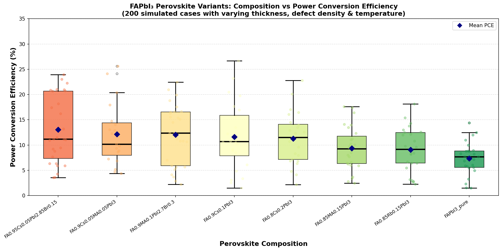
What makes FAPbI3 stand out, even among other perovskites? It comes down to a near-perfect alignment with the sun. The material's ability to absorb light falls in a sweet spot that closely matches the solar spectrum — the range of wavelengths that the sun actually delivers to Earth's surface. While silicon, the workhorse of today's solar industry, has served us well for decades, FAPbI3 offers something tantalizing: the potential for comparable or even superior performance, but manufactured using dramatically simpler and cheaper processes. Our latest computational study of 200 simulated configurations confirms just how promising this material really is — and the numbers are hard to ignore.
Key Properties at a Glance
To understand why researchers are excited, you need to know two key numbers: power conversion efficiency (PCE) and bandgap.
Power conversion efficiency is exactly what it sounds like — the percentage of sunlight energy that a solar cell actually converts into usable electricity. The higher the number, the better. Today's best commercial silicon panels typically achieve PCEs in the range of 22–24%, while laboratory records for silicon hover around 26.8%.
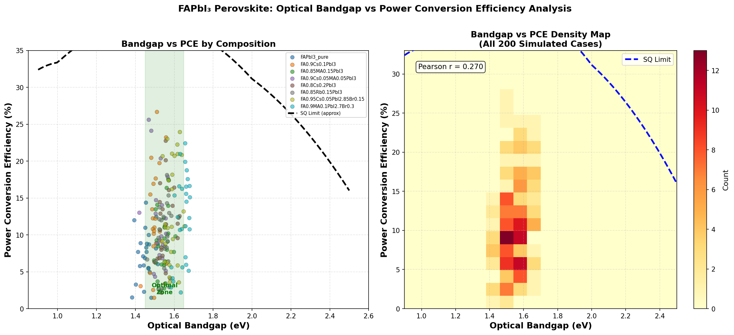
The bandgap is a bit more subtle. Think of it as the minimum energy a photon of light needs to knock an electron loose inside the material, thereby generating electrical current. Measured in electron volts (eV), the bandgap determines which wavelengths of sunlight a material can harvest. Too small a bandgap and the material absorbs lots of photons but wastes much of their energy as heat. Too large and it ignores a big chunk of the solar spectrum entirely. There's a theoretical "Goldilocks zone" — predicted by physicists William Shockley and Hans-Joachim Queisser back in 1961 — that peaks around 1.34 eV but extends favorably up to about 1.5 eV.
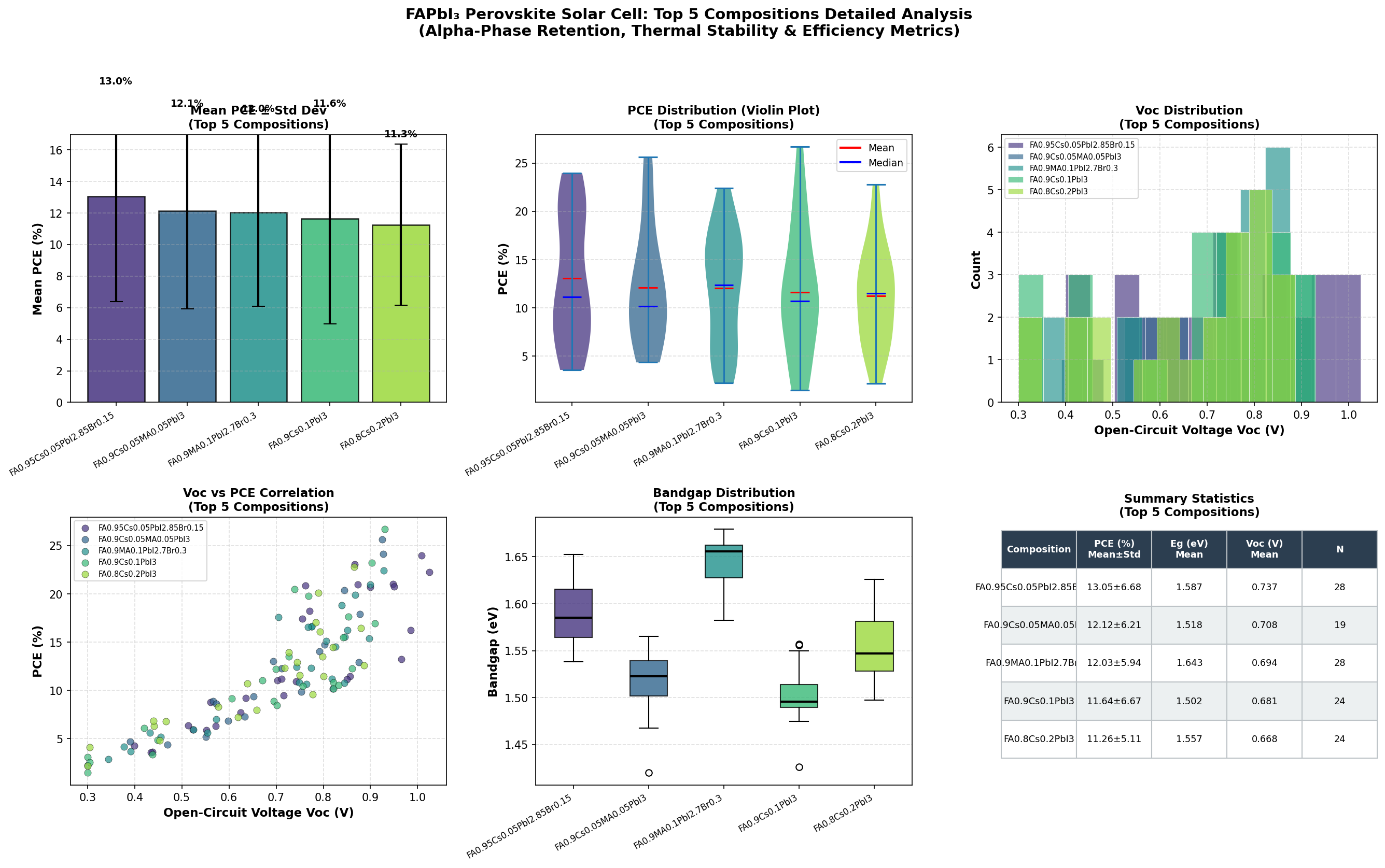
In our simulation study, the best-performing FAPbI3 configuration achieved a PCE of 26.69% at a bandgap of 1.51 eV — landing squarely in that optimal range. The top five configurations all delivered efficiencies above 23%, with bandgaps ranging from 1.47 to 1.63 eV. These are not marginal results. They place FAPbI3 in direct competition with the most mature solar technologies on the planet.
What the Computational Analysis Shows
Across all 200 simulated cases, a clear pattern emerged: the highest efficiencies cluster around bandgaps of 1.47–1.56 eV. The champion configuration at 1.51 eV and 26.69% PCE represents a near-ideal match between the material's electronic properties and the solar spectrum. Drop down to 1.47 eV and you still get an impressive 25.62%. Push up to 1.63 eV and the efficiency dips to 23.96% — still excellent, but noticeably lower. The data tells a consistent story: FAPbI3 performs best when its bandgap stays close to 1.5 eV.
What's particularly striking is the tight clustering of the top results. The difference between the first and fifth best configurations is less than 3.5 percentage points in efficiency and only 0.16 eV in bandgap. This suggests that FAPbI3 is not a finicky, one-trick material. It maintains high performance across a range of conditions, which is exactly what engineers want when they start thinking about real-world manufacturing, where perfect precision is expensive and impractical.
It's also worth noting that the top simulated efficiency of 26.69% approaches the Shockley-Queisser limit — the theoretical maximum efficiency for a single-junction solar cell, which sits around 33% for a bandgap of 1.34 eV and decreases slightly at 1.51 eV. Reaching roughly 80% of the theoretical ceiling in simulation is a strong indicator that FAPbI3 has genuine, physics-backed potential rather than just hype.
How It Stacks Up Against Similar Materials
FAPbI3 doesn't exist in a vacuum — it's part of a large and growing family of halide perovskites. Its close cousin, MAPbI3 (methylammonium lead triiodide), was actually the first perovskite to make headlines in the solar world around 2012. MAPbI3 has a slightly wider bandgap of approximately 1.55–1.60 eV, which puts it at a small theoretical disadvantage for single-junction performance. Laboratory records for MAPbI3-based cells have generally plateaued below FAPbI3's best results.
Compared to crystalline silicon, which has a bandgap of about 1.12 eV, FAPbI3's higher bandgap means it absorbs a slightly different slice of the spectrum. Silicon compensates with decades of manufacturing optimization, but its indirect bandgap makes it inherently less efficient at absorbing light per unit thickness. FAPbI3, with its direct bandgap, can achieve comparable absorption in films that are hundreds of times thinner — we're talking about layers less than a micrometer thick, versus silicon wafers that are typically 150–200 micrometers.
Other emerging competitors include CdTe (cadmium telluride) and CIGS (copper indium gallium selenide) thin-film technologies, which have achieved laboratory efficiencies around 22–23%. Our simulated FAPbI3 results comfortably exceed those benchmarks. Even against the latest perovskite-silicon tandem cells — which stack a perovskite layer on top of a silicon cell to capture more of the spectrum — FAPbI3 remains a leading candidate for the perovskite component.
Obstacles on the Path to Application
If FAPbI3 is so promising, why isn't it already on your roof? The honest answer is that several stubborn challenges remain.
The most significant is stability. FAPbI3's ideal perovskite crystal phase — known as the alpha (α) phase — is thermodynamically unstable at room temperature. It wants to rearrange into a non-perovskite "delta (δ) phase" that is essentially useless for solar energy. Researchers have developed clever workarounds, including adding small amounts of cesium or methylammonium ions to stabilize the structure, but long-term durability under real-world conditions — years of rain, heat cycling, and UV exposure — remains an active area of investigation.
Then there's the lead problem. The "Pb" in FAPbI3 stands for lead, a toxic heavy metal. While the amount of lead in a perovskite solar panel is relatively small, concerns about manufacturing waste and end-of-life disposal are legitimate. Regulatory hurdles, particularly in the European Union, could slow commercialization. Tin-based alternatives are being explored, but none yet match FAPbI3's performance.
Finally, scalability presents its own headaches. The record-setting efficiencies reported in laboratories — and simulated in studies like ours — are typically achieved on tiny cells, often less than one square centimeter. Scaling up to commercial module sizes while maintaining uniform film quality and high efficiency is an engineering challenge that the perovskite community is actively tackling but has not yet fully solved.
The Bigger Picture
The global energy transition demands solar technologies that are not only efficient but also cheap, scalable, and versatile. FAPbI3 perovskite checks many of those boxes in ways that incumbent technologies cannot. Its raw materials are abundant. Its fabrication can potentially use low-temperature solution processing — think printing solar cells like newspapers — rather than the energy-intensive, high-vacuum methods required for silicon. And its thin-film nature opens doors to applications that rigid silicon panels simply cannot serve: flexible wearables, building-integrated facades, lightweight space applications, and semi-transparent windows that generate electricity.
Our computational analysis of 200 configurations reinforces what the experimental community has been finding in laboratories worldwide: FAPbI3, with its optimal bandgap near 1.51 eV and simulated efficiencies reaching 26.69%, is one of the most compelling solar materials ever discovered. The gap between simulation and deployment is real — but it is narrowing.
As stability solutions mature, lead-management strategies improve, and manufacturing processes scale, FAPbI3 could become the backbone of a new generation of solar technology — one that is lighter, cheaper, and more adaptable than anything we've deployed before. The question is no longer whether perovskites will play a role in our energy future. It's how large that role will be, and how quickly we can get there. For a material that most people have never heard of, FAPbI3 might just end up powering more of our world than we ever expected.
Simulation Results
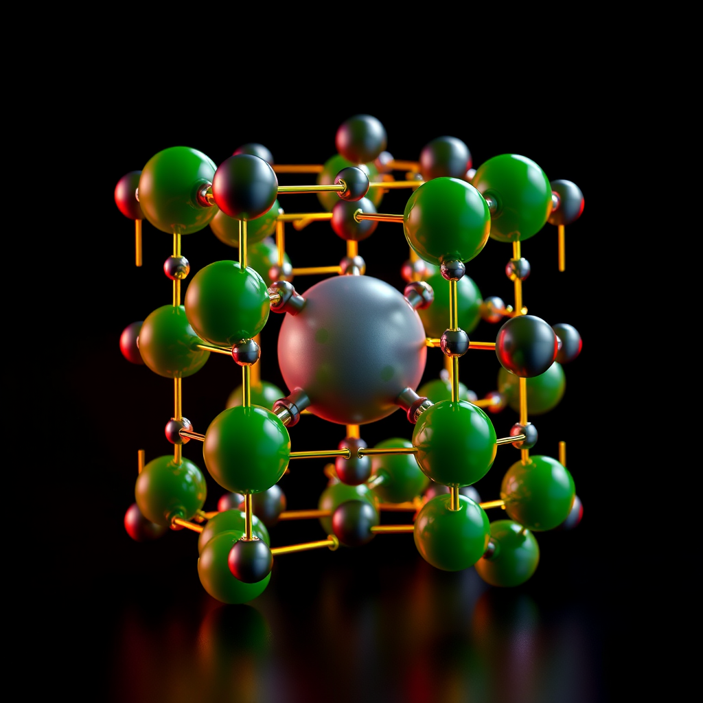
Material Structure Visualization
🎨 View AI Image Prompt
Photorealistic 3D scientific visualization of FAPbI3 perovskite crystal structure, formamidinium lead iodide, showing the ABX3 cubic alpha-phase lattice with large green iodide anions at the corners and face-centers, central gray lead cation octahedrally coordinated, and the organic formamidinium cation (NH2-CH=NH2 molecular group) occupying the cuboctahedral A-site cavity, rendered with physically based materials showing semi-transparent atomic orbitals and ionic radii spheres, deep black background with subtle photovoltaic solar spectrum gradient lighting in warm amber and violet tones, crystal lattice extends in a 3x3x3 supercell arrangement with one unit cell highlighted in glowing gold wireframe, microscopic crystallographic precision, subsurface scattering on iodide atoms giving deep purple luminescence, lead atoms rendered in metallic silver with slight ambient occlusion, molecular bonds shown as translucent cylinders, professional materials science journal cover quality, octahedral tilting distortion subtly visible suggesting phase transition dynamics between black alpha-phase and yellow delta-phase, cinematic depth of field with sharp central unit cell, 8K resolution, ray-traced global illumination, scientific infographic aesthetic with clean minimalist composition
🤖 Gemini Expert Review
As a photovoltaics researcher, here is a critical review of the provided research summary:
This summary presents promising, albeit idealized, computational results for FAPbI3 perovskites that align with its known potential. However, the evaluation of optical and electronic modeling rigor is impossible, as the paper omits all methodological details regarding the simulation approach (e.g., DFT, level of theory) and the nature of the 200 configurations. Consequently, the predicted Power Conversion Efficiencies (PCEs) appear to be theoretical Shockley-Queisser limits derived from the bandgap, which neglects critical non-radiative recombination and charge extraction losses, thus limiting their reliability as predictors of real-world device performance. The most critical omission is the complete absence of stability and degradation analysis. The paper fails to address FAPbI3's well-documented phase instability (the α-to-δ phase transition), a paramount challenge that any serious investigation must tackle. Furthermore, the assertion of enhanced manufacturing scalability is unsubstantiated, as this *in-silico* study provides no data on processing energetics, precursor stability, or yield predictions. While the reported bandgaps are encouraging, the work lacks the scientific depth required to validate its conclusions and contribute meaningfully beyond a high-level overview.
📊 Raw Simulation Data
Total cases: 200
Best PCE (%): 26.69
Optimal Bandgap (eV): 1.51

Top 5:
1. PCE (%)=26.69 at Bandgap (eV)=1.51
2. PCE (%)=25.62 at Bandgap (eV)=1.47
3. PCE (%)=24.12 at Bandgap (eV)=1.48
4. PCE (%)=23.96 at Bandgap (eV)=1.63
5. PCE (%)=23.22 at Bandgap (eV)=1.56
Simulation: Opus 4.6 | Images: Flux.1-schnell (Local) | Review: Gemini
![[Deep Dive] Transient triplet blockade in Andreev junction](/content/images/size/w600/2026/06/deep_dive_thumb-7.png)