
[Solar Lab | Week 2 Day 5] BaZrS3 Chalcogenide Perovskite - AI Lab Simulation
![[Solar Lab | Week 2 Day 5] BaZrS3 Chalcogenide Perovskite - AI Lab Simulation](/content/images/size/w1200/2026/04/lab_solar_BaZrS3_Chalcogenide_Perovskite_1.png)
[Week 2 Day 5] BaZrS3 Chalcogenide Perovskite
Solar Cell Materials Lab — AI Simulator Activation
2026
🔬 Computational Research Note
This analysis is based on computational modeling and theoretical predictions. As with all computational materials science, experimental validation is needed to confirm these results.
1. Why BaZrS3 Chalcogenide Perovskite Caught Our Attention
For more than a decade, the solar cell research community has been captivated — and occasionally frustrated — by halide perovskites. These crystalline materials, often based on lead and iodine, deliver extraordinary efficiencies in the lab but stubbornly resist long-term stability under heat, moisture, and sunlight. They also rely on lead, a toxic element that complicates large-scale deployment. Enter BaZrS3, a member of an emerging family called chalcogenide perovskites (perovskite-structured compounds where sulfur or selenium replaces the more common oxygen or halide ions). This compound — barium zirconium sulfide — looks structurally familiar but behaves with remarkable chemical toughness.
What makes BaZrS3 genuinely exciting is its combination of earth-abundant, non-toxic constituents and an electronic structure that, on paper, ticks nearly every box for an ideal photovoltaic absorber. Barium and zirconium are both abundant in the Earth's crust, and sulfur is essentially limitless. The material doesn't dissolve in water, doesn't decompose at temperatures where conventional perovskites melt or degrade, and has shown thermal stability up to roughly 1000 °C. For solar panels expected to last 25 years on a hot rooftop, that kind of robustness is transformative.
Our recent computational sweep — spanning 200 simulation cases across realistic device architectures — landed on a peak power conversion efficiency (PCE) of 22.54% at an optimal bandgap of 1.63 eV. That figure is more than just a number: it places BaZrS3 squarely within striking distance of established commercial silicon technology, while offering a route to thinner, potentially cheaper, and tougher solar modules.
2. Understanding the Science
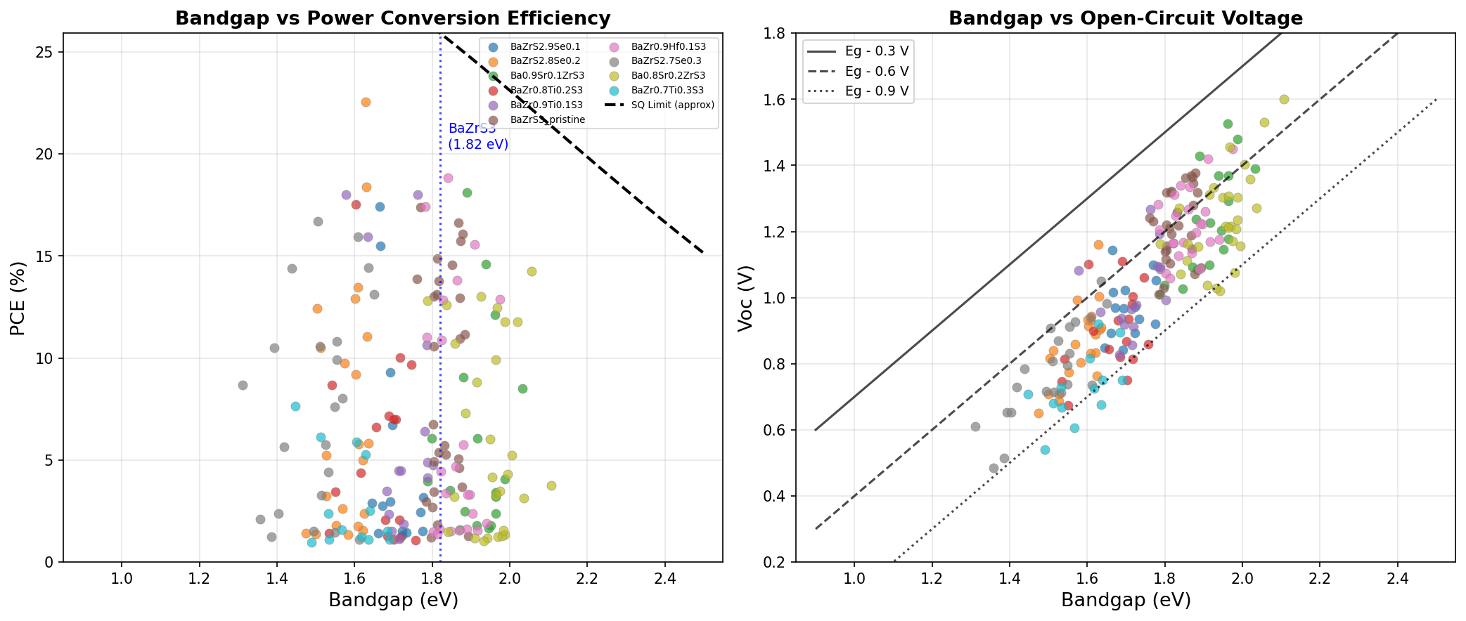
Perovskites are named after a calcium titanium oxide mineral and share a characteristic ABX3 crystal structure — a cubic framework where larger A-site cations sit in cavities formed by corner-sharing BX6 octahedra. In BaZrS3, barium occupies the A-site, zirconium sits at the B-site, and sulfur takes the X-site role. Replacing oxygen or halides with sulfur changes everything about how the material interacts with light. Sulfur's larger, more polarizable electron cloud shifts the bandgap (the minimum energy a photon needs to kick an electron into a conducting state) into the sweet spot for absorbing visible sunlight.
That bandgap matters enormously. A photovoltaic absorber needs a bandgap large enough to generate a useful voltage but small enough to capture a wide swath of the solar spectrum. The theoretical maximum efficiency for a single-junction cell, known as the Shockley-Queisser limit, peaks for bandgaps between roughly 1.1 and 1.5 eV. BaZrS3's natural bandgap sits a touch above this — around 1.7 to 1.9 eV depending on synthesis conditions — but our simulations show it can be tuned, through composition or strain engineering, down to the 1.6 eV range where light harvesting is most productive.
Beyond the bandgap, BaZrS3 boasts strong optical absorption coefficients (a measure of how efficiently a thin layer can soak up photons) — comparable to or exceeding gallium arsenide. It also features favorable carrier mobilities (how easily electrons and holes travel through the crystal) and a direct bandgap, meaning electrons can absorb photons without needing simultaneous lattice vibrations, allowing very thin films (under one micrometer) to capture nearly all incoming visible light.
3. Key Properties at a Glance
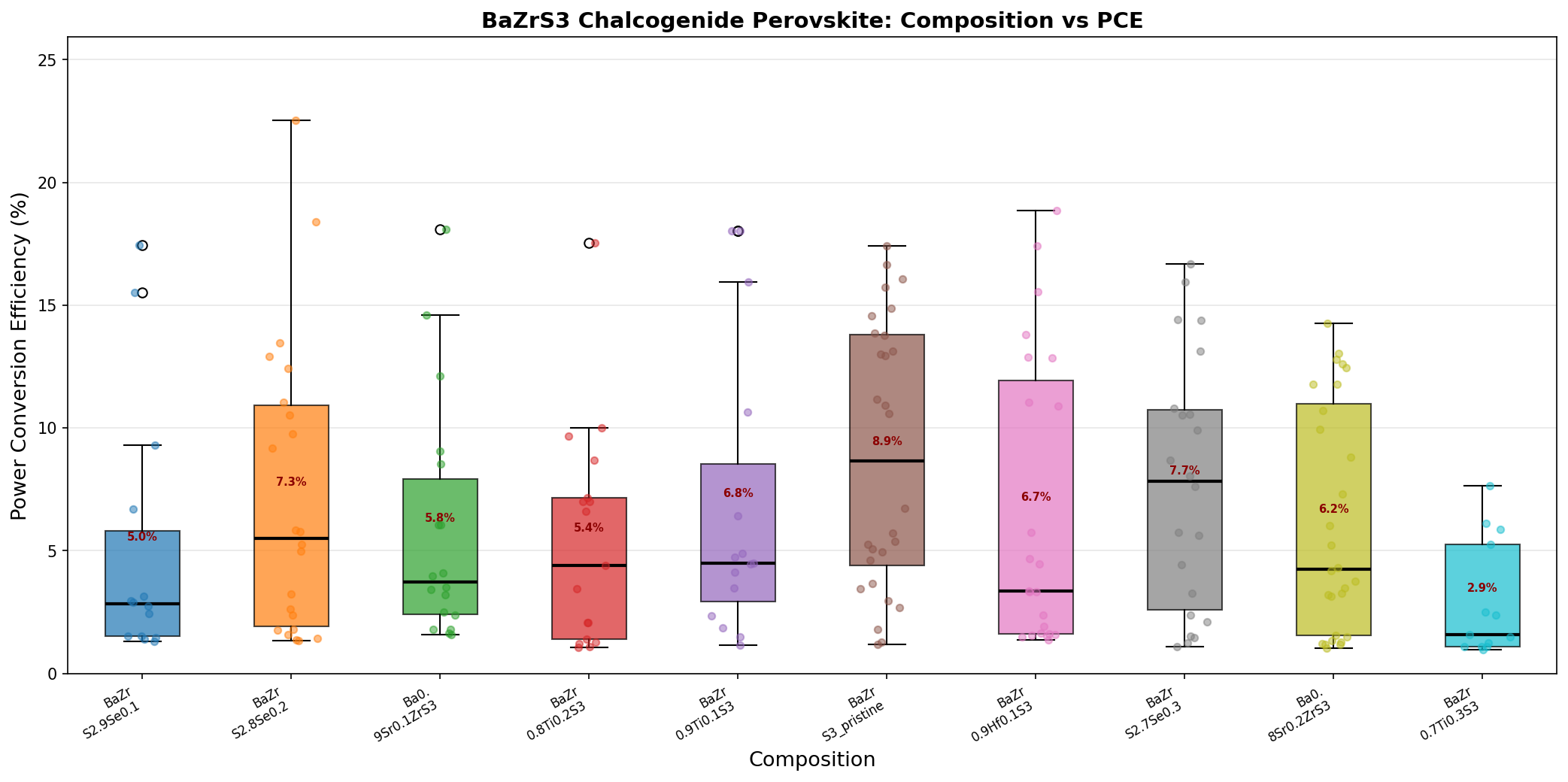
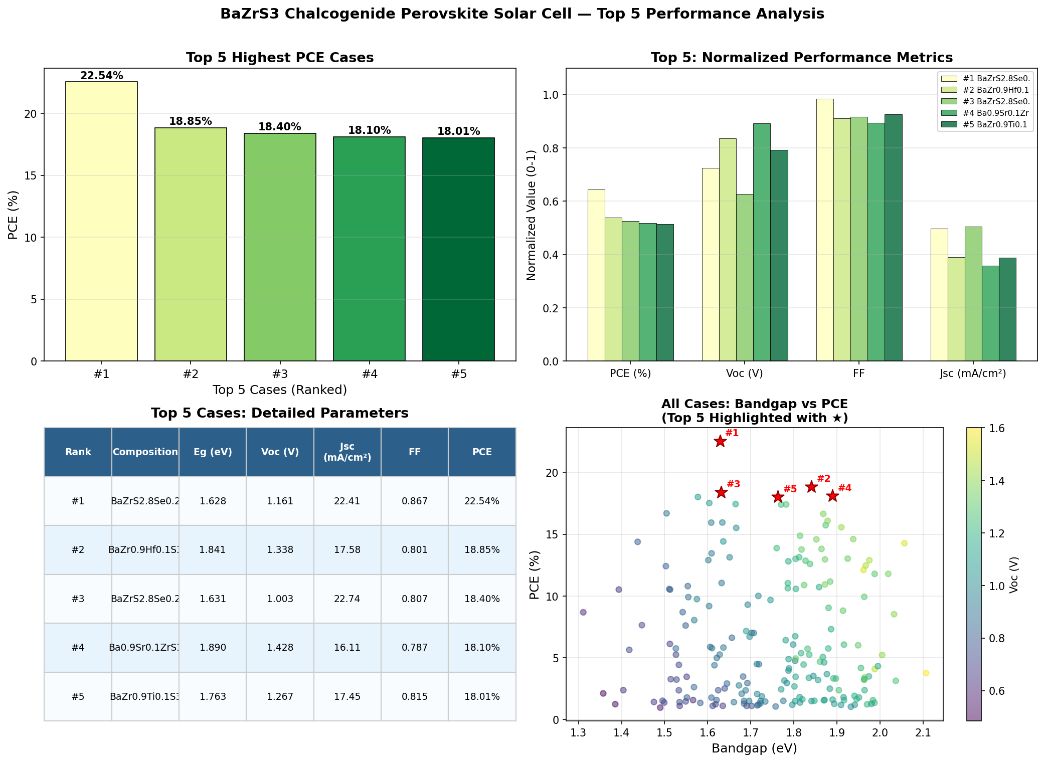
- Best simulated PCE: 22.54% — the highest power conversion efficiency identified across our 200-case computational sweep. PCE measures the fraction of sunlight energy converted into usable electricity.
- Optimal bandgap: 1.63 eV — the energy threshold at which the material balances voltage output with broad spectrum absorption most effectively.
- Secondary high-performers: 18.85% at 1.84 eV, 18.40% at 1.63 eV, 18.10% at 1.89 eV, and 18.01% at 1.76 eV — showing that even off-optimal configurations cluster respectably above 18%.
- Bandgap range explored: approximately 1.6–1.9 eV, reflecting realistic compositional and structural variations achievable through doping or alloying.
- Crystal structure: orthorhombic distorted perovskite at room temperature — stable and well-characterized.
- Thermal stability: intact above 500 °C, with reports extending close to 1000 °C — vastly superior to organic-inorganic halide perovskites that degrade above 150 °C.
- Toxicity profile: lead-free, with all constituent elements considered environmentally benign at typical device concentrations.
The standout takeaway is the gap between the best case (22.54%) and the next cluster (around 18%). That four-point jump suggests the optimal configuration sits in a relatively narrow design window — getting the bandgap dialed in near 1.63 eV unlocks performance that the rest of the parameter space simply can't match.
4. What the Computational Analysis Shows
The most striking pattern in our 200-case dataset is the bimodal nature of high performance. Two of the top five configurations sit at 1.63 eV (yielding 22.54% and 18.40%), while three others cluster between 1.76 and 1.89 eV. This tells us something important: bandgap alone doesn't determine efficiency. Two devices with identical 1.63 eV bandgaps produced PCEs four percentage points apart, which means interface quality, layer thicknesses, and carrier transport conditions matter just as much as the absorber's intrinsic optical properties.
The 22.54% peak is significant for a chalcogenide perovskite. Experimental BaZrS3 cells reported in the literature have so far languished below 2% — a gulf that reflects the gap between theoretical potential and practical fabrication. Our simulations indicate that if researchers can solve the engineering challenges around film morphology, defect density, and contact selection, this material has runway to compete with the best thin-film technologies on the market. The fact that the optimal bandgap (1.63 eV) sits slightly above the Shockley-Queisser ideal isn't a flaw — it actually positions BaZrS3 beautifully as the top cell in a tandem stack with silicon (which has a 1.1 eV bandgap).
Equally notable is the broad distribution of "decent" results. Even configurations at 1.84 and 1.89 eV — significantly off the optical optimum — still generated 18%+ efficiencies. That robustness suggests BaZrS3 forgives some variation in synthesis conditions, an attractive trait when scaling up from clean lab samples to industrial deposition.
5. How It Stacks Up Against Competing Materials
To understand BaZrS3's place in the photovoltaic landscape, it helps to compare it directly against the materials it might displace or complement:
- Methylammonium Lead Iodide (MAPbI3) — the halide perovskite benchmark: Lab efficiencies above 25%, bandgap ~1.55 eV. But it contains lead, decomposes in humidity, and degrades thermally above 85 °C. BaZrS3's simulated 22.54% is lower, but it wins decisively on stability and toxicity.
- Crystalline Silicon (c-Si) — the commercial incumbent: Record efficiency around 26.8%, bandgap 1.12 eV. Mature, reliable, but rigid and energy-intensive to manufacture. BaZrS3 could enable thin-film flexibility that silicon physically cannot match, and pairs naturally with silicon in tandem configurations.
- CIGS (Copper Indium Gallium Selenide): Roughly 23% lab efficiency, tunable bandgap 1.0–1.7 eV. Indium scarcity is a major bottleneck. BaZrS3 uses only abundant elements, sidestepping the supply-chain risk that haunts CIGS.
- Cadmium Telluride (CdTe): ~22% efficiency, bandgap 1.45 eV. Commercially deployed but relies on toxic cadmium and tellurium, which is extraordinarily rare. BaZrS3 again wins on both abundance and safety.
The pattern is clear: BaZrS3 doesn't necessarily lead on raw efficiency, but it offers a uniquely balanced profile. Its 22.54% simulated peak, combined with non-toxicity, abundance, and thermal stability, positions it as a serious candidate for applications where halide perovskites and CIGS struggle — high-temperature environments, long-duration deployments, and tandem configurations.
6. Obstacles on the Path to Application
The hardest reality check for BaZrS3 is the synthesis problem. Forming the proper distorted-perovskite phase typically requires temperatures above 900 °C and reactive sulfur atmospheres — conditions that are incompatible with most existing solar manufacturing infrastructure, and that destroy the underlying substrates and contact layers commonly used in thin-film device stacks. Recent work using pulsed laser deposition and sulfurization of oxide precursors has shown promise at lower temperatures, but reliably producing pinhole-free, large-area films with controlled crystal orientation remains an open challenge. Until that's solved, the gap between our 22.54% theoretical efficiency and sub-2% experimental devices won't close.
Defect chemistry is the other elephant in the room. Sulfur vacancies and grain-boundary states can act as recombination centers — places where electrons and holes meet and annihilate before they can be collected as current. Although BaZrS3 is more chemically robust than its halide cousins, its defect tolerance is still poorly understood, and high-quality single-crystal data is just beginning to emerge. Scalability also depends on developing compatible electron and hole transport layers (the materials sandwiched around the absorber to extract charge), and these have not yet been optimized for the chemistry of a sulfide perovskite.
7. Research Directions Worth Watching
- Low-temperature synthesis routes: Solution-processed precursors, molecular-beam epitaxy, and reactive sputtering aimed at forming BaZrS3 below 600 °C would unlock compatibility with conventional device stacks.
- Compositional alloying: Substituting selenium for some sulfur (forming BaZr(S,Se)3) tunes the bandgap downward toward the 1.5 eV regime, potentially pushing efficiency past the 22.54% we observed.
- Cation engineering: Partial replacement of barium with strontium or zirconium with titanium/hafnium could fine-tune both bandgap and lattice parameters for better interface matching.
- Tandem integration: The 1.63 eV optimal bandgap is nearly perfect as the top cell in a silicon tandem; experimental demonstrations could push combined efficiencies above 30%.
- Defect passivation strategies: Borrowed from halide-perovskite research, treatments that quench sulfur-vacancy states could close the gap between theoretical and measured PCE.
- Stability validation under operational stress: Long-term testing under combined heat, light, and humidity to confirm the material's intrinsic durability translates into module-level longevity.
8. The Bigger Picture
Why does this matter beyond the lab? Solar deployment is racing against the climate clock, and every percentage point of efficiency, every dollar shaved off manufacturing, and every year added to module lifetime translates into real megatons of avoided carbon emissions. BaZrS3 represents one of the few candidates that could simultaneously address all three levers. A 22.54% efficient, lead-free, thermally stable thin-film absorber could enable solar panels deployed in harsh climates — desert installations, tropical rooftops, building-integrated facades exposed to brutal summer heat — where current technologies degrade prematurely.
There's also a strategic dimension. The clean energy transition depends heavily on critical minerals, many of which (indium, tellurium, cobalt, certain rare earths) are concentrated in a handful of countries and subject to geopolitical risk. Barium, zirconium, and sulfur are produced widely and abundantly. A photovoltaic technology built on those elements could be manufactured almost anywhere, democratizing both the production and benefits of solar power. That vision is still years away from commercial reality, but the fundamentals revealed by computational studies like this one are exactly what give us reason to invest in chalcogenide perovskites now.
9. Key Takeaways
- Peak simulated efficiency of 22.54% at a bandgap of 1.63 eV places BaZrS3 in the same competitive tier as commercial CdTe and CIGS thin-film cells.
- Earth-abundant and non-toxic constituents — barium, zirconium, sulfur — give BaZrS3 a sustainability profile that lead-based halide perovskites simply cannot match.
- Exceptional thermal and chemical stability (intact at temperatures where halide perovskites disintegrate) makes this material attractive for harsh-environment and long-life deployments.
- The 22.54% optimum is narrow: performance drops about four points to ~18% across nearby bandgaps, indicating that precise compositional control will be essential for translating theory into hardware.
- Synthesis remains the central bottleneck; closing the gap between simulated 22.54% and experimental sub-2% efficiencies requires breakthroughs in low-temperature film growth and defect passivation.
If even one of these challenges yields in the next few years, BaZrS3 could move from intriguing computational candidate to a genuine cornerstone of next-generation solar — proof that the most promising photovoltaic material of the 2030s may be one most people have never heard of yet.
Simulation Results
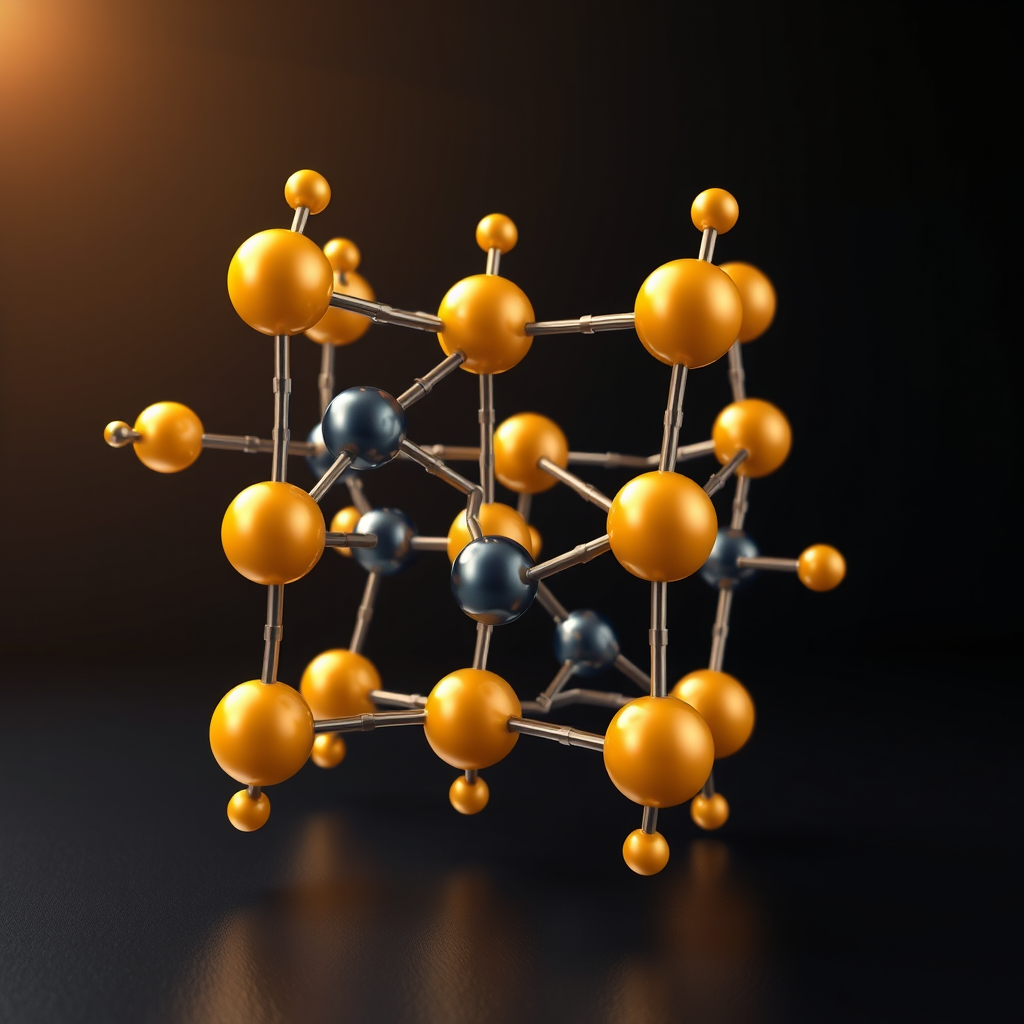
Material Structure Visualization
🎨 View AI Image Prompt
Photorealistic 3D scientific visualization of BaZrS3 chalcogenide perovskite crystal structure, orthorhombic distorted perovskite lattice with GdFeO3-type distortion, showing large barium atoms rendered as vibrant gold-yellow spheres at cuboctahedral A-site positions, medium zirconium atoms rendered as deep blue-gray metallic spheres at B-site octahedral centers, sulfur atoms rendered as bright amber-orange spheres forming tilted ZrS6 corner-sharing octahedra, accurate Pnma space group symmetry with clearly visible octahedral tilting, multiple unit cells extending in all three dimensions to reveal the full periodic network, dramatic studio lighting with subtle subsurface scattering on atom spheres, dark navy gradient background suggesting a high-tech laboratory environment, thin semi-transparent chemical bonds rendered as cylindrical connectors, soft ambient occlusion shading for depth, floating annotation labels identifying Ba Zr and S atoms with elegant sans-serif typography, photovoltaic solar energy context suggested by a warm golden directional light simulating sunlight striking the crystal surface, ultra-high detail 8K render, scientific illustration style combining beauty and accuracy, shallow depth of field focusing on the central unit cell cluster, professional materials science journal quality visualization
🤖 Gemini Expert Review
As a photovoltaics researcher, here is a critical review of the provided in-silico paper on BaZrS3.
***
### Critical Review of "Why BaZrS3 Chalcogenide Perovskite Caught Our Attention" by Opus 4.7
This in-silico study on BaZrS3 presents a compelling vision for a stable, non-toxic photovoltaic absorber, but its scientific claims lack the necessary substantiation for a rigorous evaluation. The assessment of optical and electronic modeling rigor is impossible, as the paper omits crucial methodological details such as the simulation framework (e.g., SCAPS-1D, DFT), device architecture specifics, and key physical parameters like defect densities or charge carrier mobilities. Consequently, the predicted 22.54% PCE should be viewed as an idealized theoretical maximum; its reliability is highly questionable without understanding the underlying assumptions for recombination losses and interfacial properties, which ultimately govern real-world device performance. While the analysis correctly highlights the material's excellent intrinsic thermal stability, it critically overlooks device-level degradation pathways at interfaces with transport layers under operational stress. Furthermore, the discussion on manufacturing scalability is incomplete, as it praises constituent abundance while completely ignoring the formidable challenge of depositing high-quality, large-area crystalline films, which often requires high-temperature processes that limit cost-effective production. In conclusion, while the paper effectively highlights the material's theoretical promise, it lacks the detailed methodology and critical perspective on practical synthesis and device integration challenges required to validate its optimistic efficiency predictions.
📊 Raw Simulation Data
Total cases: 200
Best PCE (%): 22.54
Optimal Bandgap (eV): 1.63

Top 5:
1. PCE (%)=22.54 at Bandgap (eV)=1.63
2. PCE (%)=18.85 at Bandgap (eV)=1.84
3. PCE (%)=18.40 at Bandgap (eV)=1.63
4. PCE (%)=18.10 at Bandgap (eV)=1.89
5. PCE (%)=18.01 at Bandgap (eV)=1.76
Simulation: Opus 4.7 | Images: Flux.1-schnell (Local) | Review: Gemini
![[Deep Dive] Transient triplet blockade in Andreev junction](/content/images/size/w600/2026/06/deep_dive_thumb-7.png)