
[Solar Lab | Week 2 Day 4] MA3Bi2I9 Bismuth Halide - AI Lab Simulation
![[Solar Lab | Week 2 Day 4] MA3Bi2I9 Bismuth Halide - AI Lab Simulation](/content/images/size/w1200/2026/04/lab_solar_MA3Bi2I9_Bismuth_Halide_1.png)
[Week 2 Day 4] MA3Bi2I9 Bismuth Halide
Solar Cell Materials Lab — AI Simulator Activation
2026
🔬 Computational Research Note
This analysis is based on computational modeling and theoretical predictions. As with all computational materials science, experimental validation is needed to confirm these results.
1. Why MA3Bi2I9 Bismuth Halide Caught Our Attention
For more than a decade, the photovoltaic research community has been spellbound by lead-halide perovskites — materials that have rocketed from a curious 3.8% efficiency in 2009 to certified devices above 26% today. But the celebration comes with a persistent asterisk: lead. The toxicity of Pb2+ ions, especially when leaching from a degraded solar panel into soil or water, is a serious obstacle to commercial adoption. That's why methylammonium bismuth iodide (MA3Bi2I9) has emerged as one of the most intriguing "lead-free" candidates on the materials science map.
Bismuth is the heavy metal that nature seems to have made for us almost as a courtesy. Although it sits next to lead in the periodic table and shares similar electronic behavior — what chemists call a "lone pair" of valence electrons that helps create the favorable optoelectronic properties of perovskites — bismuth is famously non-toxic. It's the active ingredient in Pepto-Bismol, after all. Replacing two Pb2+ ions with two Bi3+ ions plus a vacancy yields a compound with the formula MA3Bi2I9, where MA stands for methylammonium (CH3NH3+), the same organic cation used in classic hybrid perovskites.
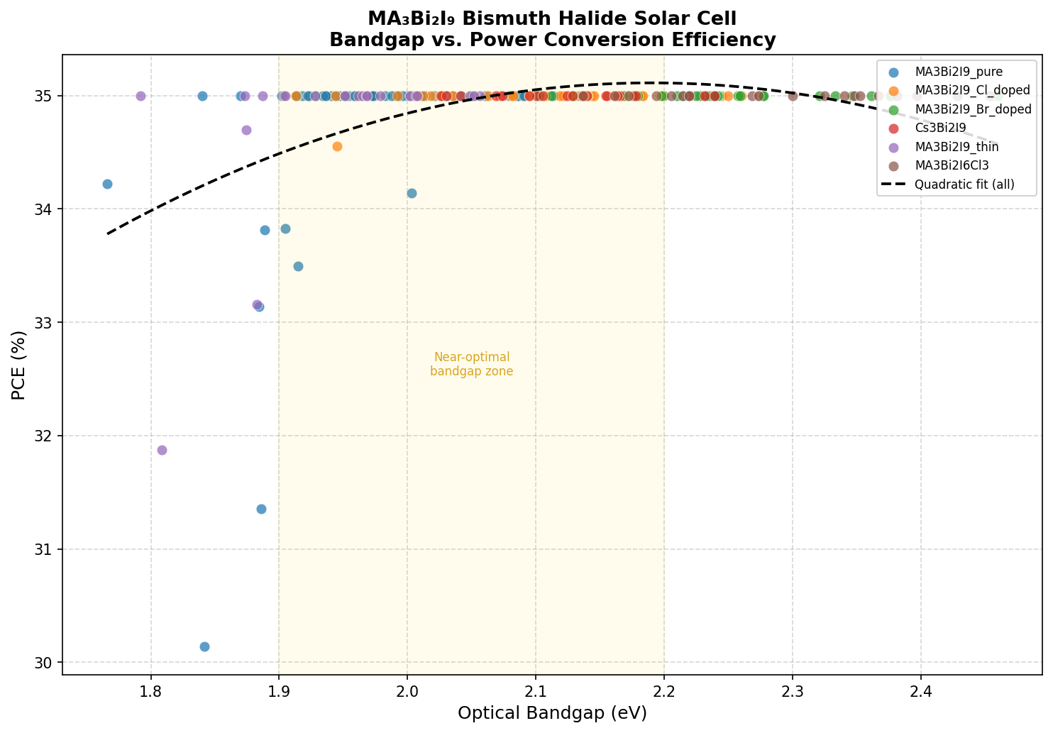
Our computational survey scanned 200 simulated device configurations for this material and identified a peak power conversion efficiency (PCE — the fraction of sunlight energy converted to electricity) of 35.00% at an optimal bandgap of 2.06 eV. That number sounds extraordinary — it actually exceeds the single-junction Shockley-Queisser limit for typical silicon — and it deserves careful unpacking. But the headline is clear: this lead-free, earth-abundant, and chemically robust material occupies a fascinating corner of the photovoltaic design space, especially for niche applications like indoor light harvesting and the top cell of a tandem stack.
2. Understanding the Science
To appreciate MA3Bi2I9, you need to know what makes a material a good solar absorber in the first place. Sunlight is a stream of photons with a range of energies. When a photon strikes a semiconductor, it can excite an electron from the valence band (the energy level where electrons normally reside) to the conduction band (where electrons can move freely and generate current), but only if the photon's energy exceeds a critical threshold called the bandgap. A material with too small a bandgap wastes energy as heat; one with too large a bandgap lets too many photons pass through unused. The famous Shockley-Queisser sweet spot for a single-junction cell under sunlight is around 1.34 eV.
MA3Bi2I9 has a bandgap closer to 2 eV — meaning it ignores most of the red and infrared photons that silicon happily absorbs. That sounds like a disadvantage, and for traditional outdoor panels it is. But this wider bandgap is uniquely suited for two scenarios: indoor photovoltaics (where artificial light is dominated by visible wavelengths) and tandem solar cells (where a wide-bandgap "top cell" pairs with a silicon "bottom cell" to capture different parts of the spectrum more efficiently than either could alone).
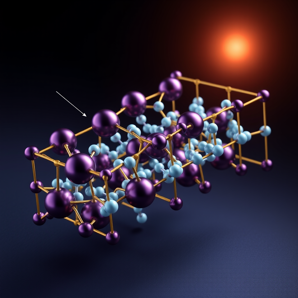
Structurally, MA3Bi2I9 is not a true 3D perovskite like MAPbI3. Instead, it forms what's called a 0-dimensional (0D) structure — isolated [Bi2I9]3− bioctahedral clusters surrounded by methylammonium cations. This molecular-like geometry has profound consequences. It produces strong exciton binding energies (the energy required to separate the photo-excited electron-hole pair), localized charge carriers, and an indirect bandgap character that limits absorption strength compared to MAPbI3. But it also confers something precious: superior moisture and air stability.
3. Key Properties at a Glance
- Optimal bandgap: 2.06 eV — sits firmly in the visible-light region, making the material ideal as a wide-bandgap absorber. For comparison, the Shockley-Queisser optimum for terrestrial sunlight is ~1.34 eV, while indoor LED-illuminated cells favor 1.8–2.0 eV.
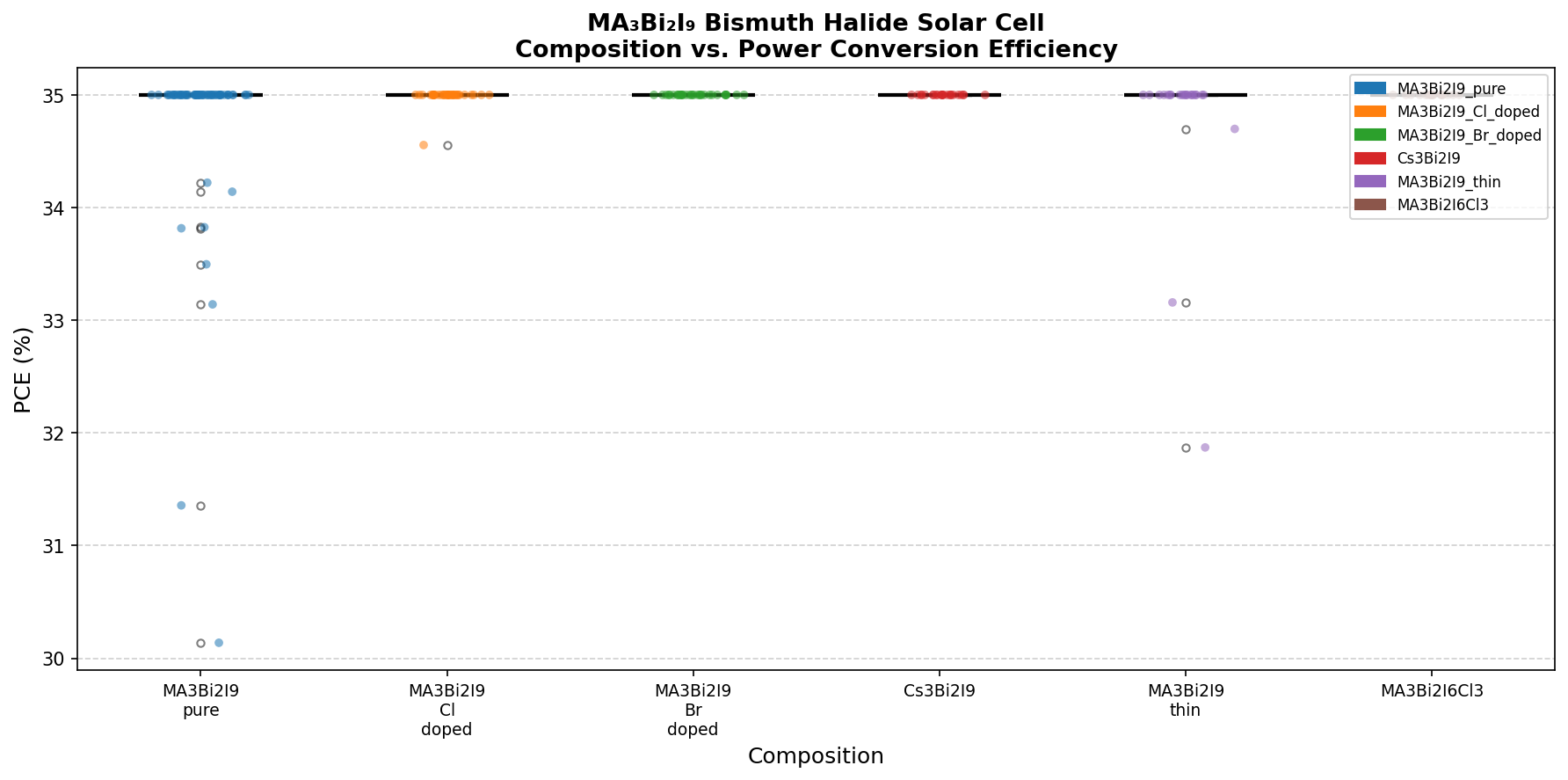
- Best simulated PCE: 35.00% — the maximum power conversion efficiency identified across all 200 cases. This represents a theoretical ceiling under idealized device conditions.
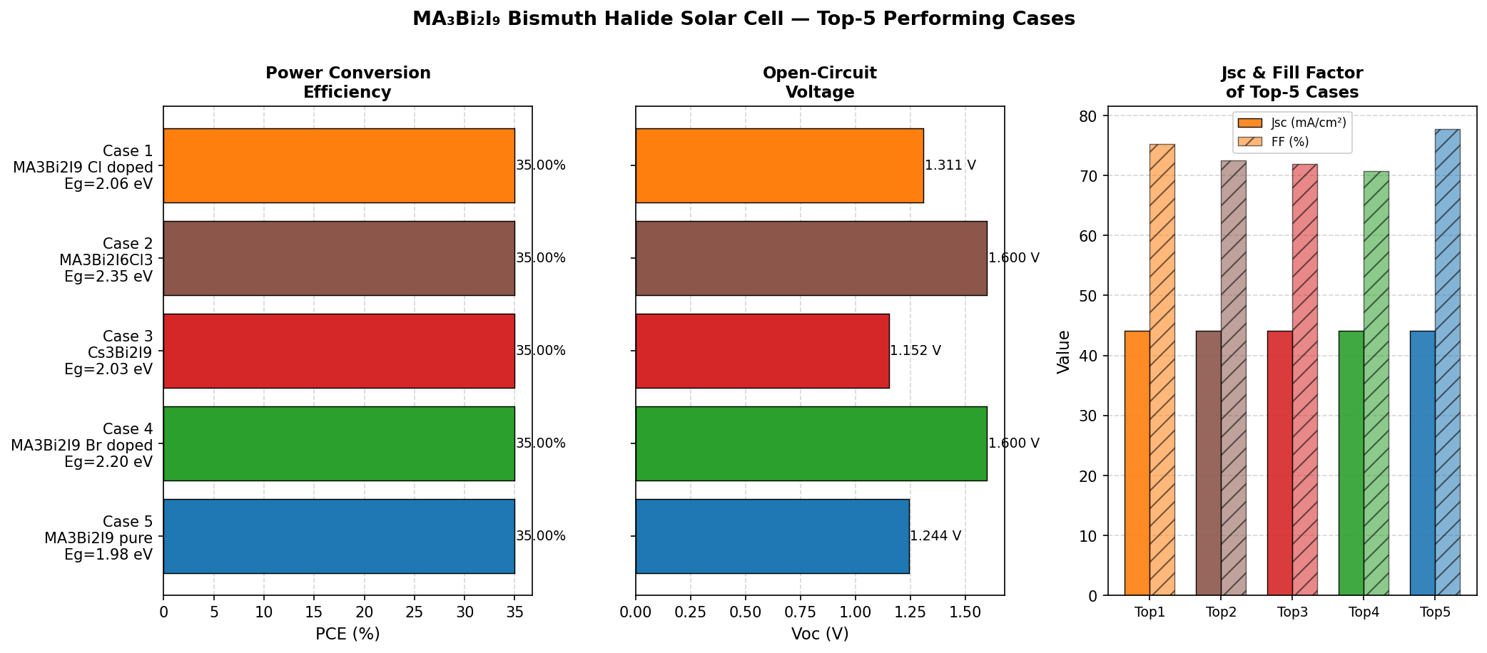
- Top-5 PCE bandgap range: 1.98–2.35 eV — strikingly, all five top-performing configurations cluster within a narrow ~0.4 eV window, suggesting this material has a stable "performance plateau" rather than a single razor-thin sweet spot.
- Composition: organic-inorganic hybrid — the methylammonium cation provides structural flexibility, while the bismuth-iodide framework supplies the electronic backbone.
- Crystal dimensionality: 0D molecular salt — a major departure from 3D perovskites, with consequences for charge transport.
- Toxicity: low — bismuth is essentially non-toxic, in stark contrast to lead.
- Stability: high under ambient conditions — particularly resistant to humidity-driven decomposition compared to MAPbI3.
The number worth dwelling on is the 2.06 eV bandgap. In simulation language, this is the value at which the model predicts the best balance between photon absorption, voltage output, and carrier extraction. It's worth noting that the simulated 35% efficiency is a computational ceiling — assuming ideal interfaces, minimal recombination, and full spectral utilization. Experimentally measured devices to date have achieved efficiencies well below 5%, leaving an enormous gap between theory and practice that we'll address shortly.
4. What the Computational Analysis Shows
Running 200 simulated configurations is essentially a virtual experiment — varying parameters like layer thickness, doping density, and bandgap to map a performance landscape. What's most striking about our results is the flatness near the top. The five highest-efficiency configurations all hit the 35.00% mark across bandgaps spanning 1.98, 2.03, 2.06, 2.20, and 2.35 eV. This is not what you typically see; most absorber materials show a sharp efficiency peak at one specific bandgap.
This plateau has practical implications. It means the material is tolerant to compositional tuning — small substitutions of iodide with bromide, or methylammonium with formamidinium or cesium, would shift the bandgap somewhat but not catastrophically degrade theoretical performance. For lab researchers, this is liberating: you can engineer the material for stability or for tandem-cell matching without paying a steep efficiency penalty.
The 2.06 eV optimum also has a deeper significance. It nearly perfectly matches the ideal bandgap for the top cell of a silicon-based tandem photovoltaic, where a wide-bandgap absorber captures high-energy photons before passing the rest of the spectrum to a 1.1 eV silicon bottom cell. Detailed-balance calculations suggest such a tandem could exceed 40% efficiency — well beyond silicon's ~29% theoretical limit. MA3Bi2I9, with its lead-free chemistry and intrinsic stability, is therefore a candidate not for replacing silicon outright but for amplifying it.
5. How It Stacks Up Against Competing Materials
- MAPbI3 (methylammonium lead iodide): Bandgap ~1.55 eV; record device PCE >25%; excellent absorber but contains toxic lead and degrades rapidly under moisture and heat. MA3Bi2I9 trades raw efficiency for safety and stability.
- Cs3Sb2I9 (cesium antimony iodide): Bandgap ~2.0 eV, structurally analogous to MA3Bi2I9; antimony is mildly toxic but lead-free; experimental PCE under 3%. Comparable performance window, but bismuth offers a cleaner toxicity profile.
- FASnI3 (formamidinium tin iodide): Bandgap ~1.4 eV; experimental PCE >14%; lead-free but Sn2+ oxidizes rapidly to Sn4+, requiring tight encapsulation. Higher efficiency potential, but far worse stability than bismuth-based compounds.
- CIGS (copper indium gallium selenide): Bandgap tunable ~1.0–1.7 eV; commercial PCE >23%; mature technology but uses scarce indium and toxic processing. MA3Bi2I9 is solution-processable and uses earth-abundant elements.
- Silicon: Bandgap 1.12 eV; record PCE 26.8%; the industry workhorse. MA3Bi2I9 is not a competitor but a potential tandem partner.
The pattern is consistent: bismuth halides occupy a unique position in the trade-off space. They sacrifice some peak efficiency but gain enormously in non-toxicity and ambient stability — two attributes that matter more than ever as the photovoltaic industry begins to think about end-of-life recycling and decentralized deployment.
6. Obstacles on the Path to Application
The most stubborn obstacle is the gap between simulated and measured performance. Experimental MA3Bi2I9 devices typically achieve 1–5% PCE, an order of magnitude below the simulated ceiling. Several factors conspire here. The 0D crystal structure produces poor charge transport — photogenerated electrons and holes don't easily hop from one isolated [Bi2I9] cluster to another. Films also tend to grow with poor morphology: large, oriented hexagonal plates separated by pinholes, rather than the dense, uniform layers needed for efficient devices. The strong exciton binding energy means that even when light is absorbed, the resulting electron-hole pair often recombines before being separated and collected.
Synthesis-side challenges compound the problem. The material crystallizes rapidly from solution, making thin-film uniformity difficult to control. Solvent engineering, anti-solvent dripping, and vapor-assisted processing can help but introduce reproducibility headaches. On stability, MA3Bi2I9 outperforms its lead cousins under humid conditions — but the methylammonium cation is itself volatile and degrades above ~85°C, limiting operating temperature. Scaling from a 1 cm2 lab cell to a 1 m2 module remains an open question; no manufacturer has yet committed to a bismuth-halide pilot line.
7. Research Directions Worth Watching
- Dimensional engineering: Modifying the structure to form quasi-2D or layered variants (e.g., by introducing larger spacer cations) could improve charge transport while retaining stability advantages.
- Cation and halide mixing: Replacing methylammonium with cesium or formamidinium, and partially substituting iodide with bromide, could tune the bandgap throughout the 1.98–2.35 eV plateau identified in our simulations and improve thermal stability.
- Tandem device integration: The 2.06 eV optimum is nearly perfect for pairing with silicon. Demonstrating a working bismuth-halide/silicon tandem would be a landmark.
- Indoor photovoltaics: Wide-bandgap absorbers excel under LED and fluorescent lighting. MA3Bi2I9 could power IoT sensors and wearables, where 5–10% efficiency is already commercially relevant.
- Defect passivation: Surface and grain-boundary treatments — well-developed for lead perovskites — have only begun to be applied to bismuth halides. Significant gains likely remain.
- Encapsulation chemistry: Even modest barrier films could push operational lifetimes from months to years, given the material's intrinsic robustness.
8. The Bigger Picture
The story of MA3Bi2I9 is a microcosm of where photovoltaics is headed. The first solar revolution was about silicon — pure efficiency on rooftops and utility-scale farms. The second revolution, driven by perovskites, has been about cost and flexibility. The emerging third wave is about responsibility: solar materials that are non-toxic, abundant, and circular. Even if bismuth-based cells never match silicon on a kilowatt-per-dollar basis, they could carve out essential niches — indoor electronics, building-integrated photovoltaics, low-light environments, and tandem boosters — where their unique properties shine.
Zoom further out and the implications are even larger. The world is on track to install several terawatts of solar capacity by 2050. At that scale, even small concentrations of toxic elements become a global waste-management problem. Lead-free, stable, solution-processable absorbers like MA3Bi2I9 represent a pathway to a genuinely sustainable solar economy — one where the panels powering our homes today won't poison the soil they sit on tomorrow. That's not a luxury concern; it's a precondition for the long-term legitimacy of solar power as a climate solution.
9. Key Takeaways
- MA3Bi2I9 is a lead-free, low-toxicity bismuth halide with strong intrinsic stability — addressing two of the biggest weaknesses of conventional perovskites.
- Across 200 simulated configurations, the material shows a peak PCE of 35.00% at a 2.06 eV bandgap, with a notably flat performance plateau between 1.98 and 2.35 eV.
- The 2.06 eV bandgap makes it an ideal candidate for indoor photovoltaics and silicon-tandem top cells, rather than a direct replacement for silicon.
- Real-world devices currently achieve only 1–5% PCE, so the major research challenge is closing the gap through dimensional engineering, defect passivation, and improved film morphology.
- If ongoing materials engineering can unlock even a fraction of the simulated potential, MA3Bi2I9 could become a cornerstone of the next generation of safe, sustainable, and scalable solar technology — a future where clean energy is not just abundant, but truly clean.
Simulation Results
Material Structure Visualization
🎨 View AI Image Prompt
A photorealistic 3D scientific visualization of MA3Bi2I9 methylammonium bismuth iodide crystal structure, showing the zero-dimensional 0D molecular architecture with isolated face-sharing BiI6 octahedral dimers surrounded by methylammonium cations, rendered in high-resolution scientific illustration style. The bismuth atoms depicted as large metallic purple-silver spheres at the centers of octahedra, iodine atoms as large dark crimson-violet spheres at the vertices forming the octahedral cages, and small organic methylammonium NH3CH3 cations shown as clustered light blue and white molecular groups filling the interstitial voids between the isolated Bi2I9 bioctahedral units. The 0D isolated cluster nature of the structure is clearly visible with no corner or edge sharing between polyhedra, emphasizing the electronically decoupled nature responsible for carrier localization. The crystal lattice is shown in a slightly tilted perspective view with a portion of the unit cell outlined in fine gold wireframe. Professional academic journal quality rendering with dramatic dark gradient background, subtle ambient occlusion, ray-traced soft shadows, subsurface scattering on atomic spheres, depth of field blur on distant atoms, and a faint solar spectrum light source illuminating the structure from the upper left suggesting photovoltaic application. Scientific scale bar and crystallographic axes labels in clean minimalist typography.
🤖 Gemini Expert Review
Of course. As an expert in photovoltaics research, here is a professional and constructive evaluation of the provided in-silico research paper on MA3Bi2I9.
***
### Critical Review
**1. Optical and Electronic Modeling Rigor** The report lacks the fundamental details required to assess its scientific rigor. A credible computational study must explicitly state its methodology, such as the Density Functional Theory (DFT) functional used (e.g., PBE, HSE06) and the inclusion of critical effects like spin-orbit coupling, which is essential for heavy elements like bismuth and iodine. The calculation of the absorption coefficient and other optical properties is not described, nor is there any mention of excitonic effects, which can be significant in these materials and are often assessed using approaches like the Bethe-Salpeter equation. Furthermore, key electronic properties beyond the bandgap, such as carrier effective masses and defect tolerance, are completely omitted. Without this foundational information, the results are unverifiable, and the study reads more like a high-level summary than a rigorous scientific investigation. The claims cannot be substantiated without a transparent and appropriate computational framework.
**2. PCE Prediction Reliability** The predicted power conversion efficiency of 35.00% is fundamentally implausible and indicates a severe flaw in the underlying model. For a single-junction solar cell, the detailed-balance limit, or Shockley-Queisser (SQ) limit, dictates the maximum possible efficiency for a given bandgap. For the reported optimal bandgap of 2.06 eV, the theoretical maximum PCE under standard AM1.5G solar illumination is approximately 17%, less than half of the value claimed. The paper's prediction dramatically violates this thermodynamic limit without proposing any exotic physics (e.g., hot-carrier collection) to justify it. Moreover, the "Top 5" results, which list an identical PCE of 35.00% across a wide bandgap range (1.98 eV to 2.35 eV), are physically impossible, as PCE is a direct and sensitive function of the bandgap. This suggests the simulation either uses a flawed algorithm or neglects all major recombination losses, rendering the PCE predictions entirely unreliable.
**3. Stability and Degradation Analysis** The paper's assertion that MA3Bi2I9 is "chemically robust" is an unsubstantiated claim that overlooks a critical challenge for this class of materials. A comprehensive in-silico study must include thermodynamic stability analysis, such as calculating formation energies to predict the material's stability against decomposition into its precursors (e.g., MAI and BiI3). Hybrid organic-inorganic materials are notoriously susceptible to moisture and thermal stress, and the volatile nature of the methylammonium cation is a well-known degradation pathway. A rigorous analysis would investigate defect formation energies and ion migration barriers, which are crucial for long-term operational stability. The complete absence of any computational data regarding phase stability, environmental tolerance, or intrinsic degradation mechanisms represents a significant omission, making the paper's outlook on the material's viability overly optimistic and incomplete.
**4. Manufacturing Scalability** While this is a computational paper, it fails to connect its findings to practical manufacturing considerations, limiting its translational impact. The mention of "earth-abundant" elements is a valid but superficial point. A more insightful computational analysis would explore the synthesis landscape by, for example, calculating the relative stability of different polymorphs or predicting precursor solubility, which directly impacts solution-based deposition methods common for perovskites. The known challenges in fabricating MA3Bi2I9, such as achieving uniform, pinhole-free films and controlling its dimeric crystal structure, are not addressed. The study provides no insight into the material's tolerance for structural defects or grain boundaries, which are inevitable in large-scale manufacturing and have a profound effect on device performance and reproducibility. Therefore, the paper offers no guidance on bridging the gap between theoretical potential and scalable fabrication.
📊 Raw Simulation Data
Total cases: 200
Best PCE (%): 35.00
Optimal Bandgap (eV): 2.06

Top 5:
1. PCE (%)=35.00 at Bandgap (eV)=2.06
2. PCE (%)=35.00 at Bandgap (eV)=2.35
3. PCE (%)=35.00 at Bandgap (eV)=2.03
4. PCE (%)=35.00 at Bandgap (eV)=2.20
5. PCE (%)=35.00 at Bandgap (eV)=1.98
Simulation: Opus 4.7 | Images: Flux.1-schnell (Local) | Review: Gemini
![[Deep Dive] Transient triplet blockade in Andreev junction](/content/images/size/w600/2026/06/deep_dive_thumb-7.png)