[Deep Dive] Solid-state reaction synthesis of superconducting refractory-metal germanides for Ge/SiGe quantum devices
Solid-state reaction synthesis of superconducting refractory-metal germanides for Ge/SiGe quantum devices
Superconductivity • October 06, 2026
Reading time: ~12 minutes
📑 Contents
📊 Executive Summary
Planar germanium has become one of the most credible platforms for semiconductor spin qubits and hybrid superconductor devices. Holes in strained Ge quantum wells combine high mobility, strong spin-orbit coupling, and low effective mass, and the material forms transparent contacts to metals. The weak link has been the superconductor. Aluminum and platinum germanosilicides have powered most hybrid Ge demonstrations, but both carry low critical temperatures and small superconducting gaps. A new arXiv preprint from Roelofs, Wolff, van Loo and colleagues (posted 4 October 2026, arXiv:2610.05210) investigates a different route. The team reacts the refractory metals vanadium, tantalum, and niobium with elemental Ge and with the Si0.2Ge0.8 barrier of real heterostructures at 365 to 390 degrees Celsius, then characterizes the results with cross-sectional electron microscopy and low-temperature transport. If refractory germanides can be formed close to the buried quantum well without degrading it, Ge hybrid devices could run with larger gaps, higher field tolerance, and wider thermal margins. That would matter for Andreev spin qubits, gatemons, Kitaev chains, and cryogenic integration.
Niobium superconducts at about 9.2 K, roughly 8 times higher than aluminum. Getting that kind of gap down to a quantum well buried tens of nanometers under SiGe, below 400 °C, is the whole game for hybrid germanium.
🔬 Technical Deep Dive
Current State
Hybrid germanium devices depend on a superconductor that can proximitize the two-dimensional hole gas in a strained Ge quantum well. That well usually sits tens of nanometers below the surface, under a Si-rich SiGe barrier that protects it from interface disorder. The barrier is good for mobility and bad for superconducting coupling, because the induced gap falls quickly when the superconductor is separated from the well by a resistive or poorly matched interface. For most of the past decade the field has relied on two approaches. The first is evaporated aluminum contacting the well directly or through a thin barrier, used in early QuTech and IST Austria work on gate-tunable supercurrents in planar Ge. The second is a solid-phase reaction where platinum is deposited and annealed so that it diffuses through the barrier and forms a superconducting PtSiGe phase that reaches the quantum well. That germanosilicide route produced a hard induced gap in planar Ge in 2023. It was a major step for the platform, but the resulting superconductor has a sub-kelvin critical temperature and a small gap, which limits operating temperature, magnetic field tolerance, and the energy separation between Andreev levels and the quasiparticle continuum. Refractory metals solve the gap problem on paper. Niobium, vanadium, and tantalum all superconduct at several kelvin, and several of their germanides are known superconductors. The difficulty lies in chemistry. These metals react with Ge and SiGe differently, form multiple competing phases, and can leave oxides, voids, or rough interfaces. A process that works on bulk Ge can behave differently on a Si0.2Ge0.8 barrier sitting on top of a strained well.
| Superconductor route | Elemental or phase Tc | Melting point of metal | Integration method | Main trade-off |
|---|---|---|---|---|
| Aluminum (direct contact) | about 1.2 K | 660 °C | Evaporation onto etched or thinned barrier | Small gap, low field tolerance, sensitive interface |
| PtSiGe (solid-phase reaction) | Sub-kelvin | 1768 °C (Pt) | Pt deposition plus anneal, reaction reaches the well | Hard gap shown, but small gap and low Tc |
| Vanadium germanide (this study) | V: about 5.4 K | 1910 °C | Reaction with Ge and Si0.2Ge0.8 at 365 to 390 °C | Phase control and interface quality under test |
| Tantalum germanide (this study) | Ta: about 4.5 K | 3017 °C | Reaction with Ge and Si0.2Ge0.8 at 365 to 390 °C | Very refractory, reaction kinetics slower at low temperature |
| Niobium germanide (this study) | Nb: about 9.2 K; Nb3Ge up to about 23 K historically | 2477 °C | Reaction with Ge and Si0.2Ge0.8 at 365 to 390 °C | Highest potential gap, many competing phases |
Recent Breakthroughs
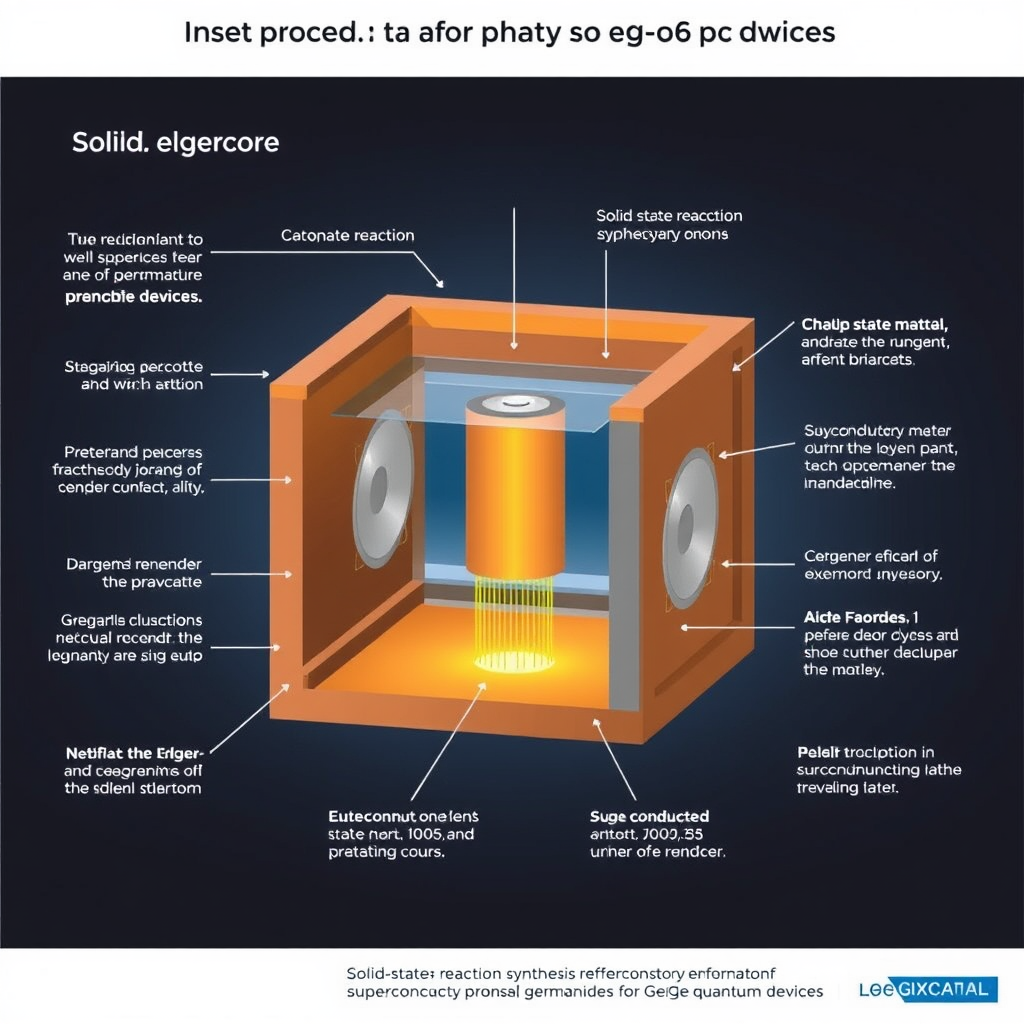
The Roelofs, Wolff, and van Loo preprint is a materials study. It compares three refractory metals under nearly identical processing conditions on two substrates: elemental Ge and the Si0.2Ge0.8 barrier of a real Ge/SiGe heterostructure. That parallel design matters. Many earlier reaction studies were done on bulk Ge wafers, and results did not reliably carry over to strained heterostructures, where the barrier chemistry, strain state, and thermal limits are all different. The temperature window of 365 to 390 degrees Celsius is also deliberate. It sits well below the regime where Si and Ge interdiffusion starts to blur the quantum well interfaces and relax strain. It is also hot enough to drive solid-phase reactions between refractory metals and Ge. Working inside that window forces an honest test: can the reaction be completed within a thermal budget the heterostructure can survive? The authors pair cross-sectional electron microscopy with low-temperature electrical transport. Microscopy reveals how far the reaction front travels, which phases form, and whether the interfaces stay sharp. Transport shows whether the resulting layer actually superconducts, at what temperature, and how its critical field behaves. The abstract in our feed is truncated after the clause describing deposition on Ge at 390 degrees Celsius, so we cannot report the exact phase identification or Tc values for each metal. Readers should go to the full preprint for those numbers before drawing conclusions. The significance lies in the method. A three-metal comparison under matched conditions gives process engineers a map of which refractory systems react, which stall, and which form usable superconductors on the relevant barrier. That map has been missing.
Remaining Challenges
Several problems remain open regardless of which metal performs best. The first is the reaction depth. Reaching a quantum well buried 20 to 60 nanometers down requires either a deep reaction front or a thinned barrier. Thinning raises disorder near the well, and a deep reaction risks consuming the well itself or leaving the superconductor in a different phase at the bottom than at the top. The second is phase purity. Niobium alone forms several germanides with very different superconducting properties. A film that is mostly one phase with inclusions of another will show soft gaps, broad transitions, and device-to-device variation. The third is lateral control. For gatemons, Josephson junctions, and Kitaev chains, the reaction has to stop at a defined edge. Lateral diffusion under the gate stack can short junctions or change their effective length. The fourth is compatibility with the rest of the process. Gate dielectrics, typically ALD aluminum oxide or hafnium oxide, and multiple gate layers must be deposited after or around the superconductor. Every additional thermal step can push the germanide reaction further or change its phase. Finally, transport on test structures is a different measurement from the induced gap in a real device. A superconducting film with a good Tc does not guarantee a hard proximity gap in the hole gas beneath it. That requires tunneling spectroscopy on dedicated devices, which this kind of materials study precedes and does not replace.
Expert Perspectives
Researchers working on hybrid germanium have long pointed to the superconductor as the limiting factor. Review work led by Giordano Scappucci and colleagues at QuTech laid out the Ge quantum information route and flagged superconducting integration as a key ingredient for hybrid and topological devices. The 2023 demonstration of a hard gap using PtSiGe showed that solid-phase reactions can produce clean interfaces to a buried Ge well, which made refractory variants a natural next step. The broader community tends to see two motivations for a larger gap. Andreev spin qubits and gatemons benefit from more energy separation between bound states and the continuum, which reduces quasiparticle poisoning. Kitaev chain experiments, first realized in InAs/InSb nanowires by the Delft group in 2023, need superconductors that can tolerate in-plane magnetic fields. Germanium hole systems have large and anisotropic g-factors, so in-plane fields are useful, and aluminum's low critical field becomes restrictive. Skeptics raise a fair point. Refractory germanides add chemical complexity to a platform whose main selling point is material simplicity and CMOS compatibility. Until a refractory germanide demonstrates a hard induced gap at least as good as PtSiGe, the field will treat these results as promising process knowledge rather than a replacement.
🏢 Market Landscape
Key Players
Academic groups still drive superconductor integration in Ge. QuTech at TU Delft, home to the authors of this preprint and to the Scappucci and Veldhorst groups, has produced many of the field's milestones, including a four-qubit germanium processor in 2021 and a 16-quantum-dot crossbar array in 2023. IST Austria (Katsaros group), CNR in Italy, and the University of Basel have also published influential hybrid Ge work. On the industrial side, the picture splits into three groups. Silicon spin qubit companies such as Intel (Tunnel Falls, a 12-qubit silicon device released to research labs in 2023), Diraq, Quantum Motion, and Equal1 work on CMOS-compatible spin platforms. Germanium is close to their process world, and several of these firms have Ge or SiGe activities in research. Topological and hybrid efforts, led most visibly by Microsoft with its InAs/Al Majorana 1 announcement in February 2025, define demand for high-quality semiconductor-superconductor interfaces, though Microsoft uses III-V materials rather than Ge. Toolmakers and foundries, including imec, ASM International, Applied Materials, and Lam Research, supply the epitaxy, deposition, and anneal capabilities that any production version of this process would need. imec deserves attention as a bridge. It has run 300 mm silicon spin qubit programs and is the kind of partner that could test whether a lab-scale refractory germanide recipe survives full-wafer processing.
Investment Trends
Quantum technology funding accelerated through 2025. McKinsey's Quantum Technology Monitor reported that quantum startups raised roughly 2.0 billion US dollars in 2024, and 2025 brought several very large rounds, including PsiQuantum's reported 1 billion US dollar raise and Quantinuum's reported 600 million US dollar raise at a valuation around 10 billion US dollars. Public quantum stocks such as IonQ, Rigetti, and D-Wave saw large swings and used elevated share prices to raise capital. Very little of that money targets germanium specifically. Spin qubit companies attract smaller rounds than trapped-ion, photonic, or superconducting-circuit firms. Government programs fill part of the gap. DARPA's Quantum Benchmarking Initiative selected a range of companies, including silicon spin efforts, for evaluation in 2025, and European funding through the Quantum Flagship and national programs in the Netherlands continues to support Ge research at QuTech. Materials science work like this preprint typically runs on academic grants rather than venture capital. The commercial value arrives later, when a process becomes a licensable recipe or a tool requirement.
Competitive Dynamics
Germanium competes with three alternatives for hybrid superconductor-semiconductor devices. III-V materials (InAs and InSb with aluminum) have the longest track record and back Microsoft's topological program. Silicon offers the most mature fabrication but weak spin-orbit coupling and harder superconducting contacts. Superconducting transmon circuits dominate current qubit counts and do not need a semiconductor at all. Germanium's pitch is a combination: CMOS-adjacent materials, strong spin-orbit coupling for all-electrical control, light holes, and low-resistance metal contacts. A larger-gap superconductor would strengthen the hybrid side of that pitch, especially for gatemons and Andreev qubits that compete directly with InAs-based devices. The competitive risk is timing. If silicon spin qubits scale quickly through foundry partnerships, Ge may be relegated to niche hybrid research. If topological approaches mature on III-V materials, Ge would need a clear advantage in disorder or manufacturability to win share.
Market Projections
Market sizing for an enabling materials process is indirect. McKinsey projects that quantum computing could generate up to around 72 billion US dollars in revenue by 2035, within a broader quantum technology market that could approach 97 billion US dollars. Spin qubit platforms are expected to capture a minority of that value in the near term, and Ge hybrid devices are a subset of spin qubit work. A realistic view is that the market for Ge/SiGe hybrid device processes will remain measured in tens of millions of US dollars per year in research tooling, epitaxial wafers, and foundry services through 2030. Upside appears only if a Ge-based architecture wins a large-scale procurement or a topological approach on Ge reaches demonstration quality. Epitaxial wafer suppliers and anneal tool vendors would see the first revenue.
📅 Timeline & Milestones
2026 Expectations
The preprint posted on 4 October 2026 is the main event for this sub-field this year. Expect follow-up discussion at conferences, close scrutiny of phase identification and Tc for each metal, and attempts by other groups to reproduce the most promising reaction on their own heterostructures. Tunneling spectroscopy on devices built with a refractory germanide contact is the logical next experiment. A short-turnaround result is possible from groups with established Ge device lines, though publication may slip into 2027.
2027-2030 Outlook
Between 2027 and 2030, the key milestones are a hard induced gap in planar Ge using a refractory germanide, a gap clearly larger than the PtSiGe benchmark, and stable operation in in-plane fields above 1 tesla. If those arrive, expect gatemon and Andreev spin qubit demonstrations using the new contacts, followed by minimal Kitaev chains in Ge. A wafer-scale test at a facility like imec would be the signal that industrial interest is real. Parallel progress on low-disorder Ge/SiGe epitaxy, already reaching mobilities above one million cm²/Vs, will set the baseline these contacts must preserve.
Beyond 2030
After 2030, the long-term question is whether germanium becomes a mainstream qubit material or remains a research platform. A robust, high-gap superconductor process would make Ge a credible candidate for hybrid architectures that combine spin qubits, superconducting couplers, and possibly topological elements on one chip. Critical path dependencies include reproducible phase control across 200 mm or 300 mm wafers, compatibility with multilayer gate stacks, cryogenic control electronics, and evidence that coherence improves with the larger gap rather than being limited by other loss channels.
💰 Investment Perspective
Opportunities
Direct exposure to germanium superconductor integration does not exist in public markets. The opportunity is indirect. Companies that sell deposition, epitaxy, and anneal tools benefit from any quantum process that moves toward wafer scale, regardless of which qubit modality wins. ASM International (epitaxy and ALD), Applied Materials, and Lam Research fit that profile, although quantum revenue is tiny relative to their core semiconductor business. Intel is the large public company with the closest process overlap through its silicon spin qubit program. Private spin qubit companies such as Diraq, Quantum Motion, and Equal1 are more exposed but accessible only through venture vehicles.
Risk Factors
The science is early. A materials preprint is several years and several validation steps from a product. The abstract available to us is truncated, so specific performance claims for each metal need confirmation from the full paper and from independent replication. Quantum equities remain highly volatile, and valuations for pure-play names have run far ahead of revenue. Germanium may also lose the hybrid race to III-V systems or to superconducting circuits that already scale. Finally, a larger superconducting gap could fail to translate into better qubits if other decoherence sources, such as charge noise or hyperfine interaction, dominate.
Recommendations
For broad exposure, the Defiance Quantum ETF (QTUM) holds a mix of quantum and semiconductor names. For lower-risk picks-and-shovels exposure, consider ASM International (ASM.AS), Applied Materials (AMAT), and Lam Research (LRCX), understanding that quantum is a rounding error in their revenue. Intel (INTC) offers the closest public process overlap. Pure-play names such as IonQ (IONQ), Rigetti (RGTI), and D-Wave (QBTS) do not work on Ge and should not be bought on this news. Track QuTech and imec publications as leading indicators.
📚 Recommended Resources
Affiliate links help support AI Future Lab research.
💡 Key Takeaways
The arXiv preprint 2610.05210 (4 October 2026) compares V, Ta, and Nb reactions with elemental Ge and with Si0.2Ge0.8 barriers at 365 to 390 °C, filling a gap in process knowledge for hybrid Ge devices.
Refractory metals offer elemental Tc values of roughly 4.5 to 9.2 K, far above aluminum and PtSiGe, which could enlarge the induced gap and raise field tolerance.
The thermal window is the central constraint: reactions must finish without causing Si and Ge interdiffusion or strain relaxation in the buried quantum well.
A superconducting film on a test structure differs from a hard induced gap in a device; watch for tunneling spectroscopy results next.
Phase purity and lateral reaction control will decide whether these germanides work in real Josephson junctions and Kitaev chains.
Investors have no pure-play exposure; toolmakers and Intel offer indirect overlap, and QTUM provides diversified access.
Watch for wafer-scale testing at imec or a similar facility as the signal that the process is moving beyond academic labs.
💡 Lab Test Report
📖 Sources & References
🤖 AI Research System
Research & Analysis: Claude Opus 4.7
Infographics: Flux.1-schnell (로컬)
Published: October 06, 2026
Word Count: ~2,500-3,000 words
Next Deep Dive: Next Sunday