[Deep Dive] Multidimensional Light Detection with Symmetry-engineered Heterojunctions
![[Deep Dive] Multidimensional Light Detection with Symmetry-engineered Heterojunctions](/content/images/size/w1200/2026/09/deep_dive_thumb-2.png)
Multidimensional Light Detection with Symmetry-engineered Heterojunctions
Applied Physics • September 06, 2026
Reading time: ~12 minutes
📑 Contents
📊 Executive Summary
Miniaturised light detection has spent a decade splitting into two camps: chips that resolve polarisation and chips that resolve wavelength. Almost nothing does both well in the same footprint. A new arXiv preprint from Yucai Lin, Yaoqiang Zhou and Ruijuan Tian (2609.02161v1, posted 2 September 2026) argues that the fix is crystallographic rather than optical: engineer the point-group symmetry of a van der Waals heterojunction so that its photocurrent tensor carries linear polarisation, circular polarisation and spectral information simultaneously, then unmix them computationally. That matters because the circular channel (Stokes S3) is the one commercial polarisation sensors still cannot capture without bolting on retarders. Over the past quarter the surrounding ecosystem has moved fast: Metalenz continues pushing meta-optic polarisation sensing into phone-grade authentication, computational spectrometer papers keep shrinking resolution below 10 nm from single detectors, and hyperspectral imaging remains a roughly 17 percent CAGR market. The technology is real, early, and calibration-hungry.
The device stops being a detector in the classical sense and becomes a physical encoder: the optical bench collapses into the pixel, and the calibration burden moves into software.
🔬 Technical Deep Dive
Current State
Light carries at least four independently useful dimensions: intensity, wavelength, linear polarisation state and handedness. Commercial silicon captures the first well, the second through filters, the third through micro-polariser arrays, and the fourth almost never. Sony's Polarsens family put a four-orientation wire-grid block over 3.45 um pixels back in 2018 and it still defines the volume market. Those blocks recover S0, S1 and S2. Circular polarisation, S3, requires a quarter-wave retarder in the stack or a genuinely chiral optical element, and neither survives a cost-down BOM review easily.
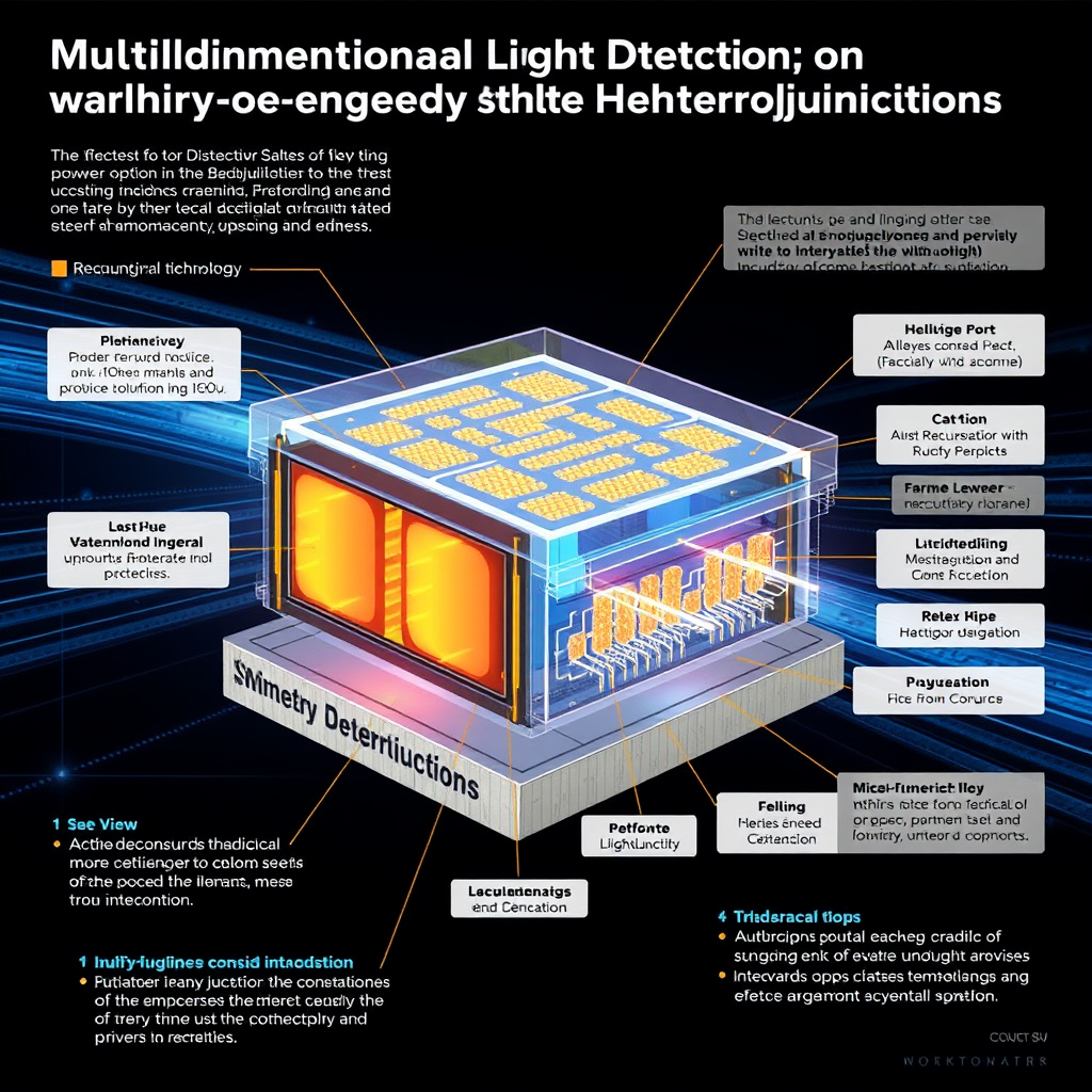
The symmetry-engineering route attacks this from materials physics instead. In a crystal with broken inversion symmetry, illumination generates a bulk photovoltaic current whose direction and magnitude depend on the polarisation state through a third-rank photoconductivity tensor. Restrict the point group further, into a gyrotropic class, and the circular photogalvanic effect appears: the photocurrent flips sign with handedness. Tellurium, GeS, GeSe, ReS2 and twisted bilayer stacks all sit in useful symmetry classes. Build a heterojunction from those layers and you also get a built-in field, so the device runs at zero bias with low dark current, and the band alignment gives you a bias-tunable spectral response that doubles as an encoding basis for computational spectral reconstruction. One diode, four unknowns, multiple measurement channels.
| Approach | Linear (S1, S2) | Circular (S3) | Spectral info | Extra optics | Bias needed | Maturity |
|---|---|---|---|---|---|---|
| Micro-polariser DoFP (Sony IMX250MZR) | Yes | No | None (mono) or RGB Bayer | Wire-grid array | Standard CMOS rails | Volume production |
| Metasurface full-Stokes camera (Capasso-style matrix Fourier optics) | Yes | Yes | Narrowband, dispersion-limited | Nanostructured meta-optic + sensor | Standard CMOS rails | Early commercial |
| Reconstructive single-detector spectrometer | No | No | Yes, sub-10 nm typical | None, algorithm-based | Bias sweep required | Lab to pilot |
| Low-symmetry 2D photodiode (linear anisotropy) | Yes | Weak or none | Limited | None | Often zero bias | Lab |
| Symmetry-engineered heterojunction (this work) | Yes | Yes, intrinsic CPGE | Yes, via bias-tuned response basis | None | Bias sweep for spectral channel | Lab demonstration |
The table makes the trade obvious. Every row above the last buys a dimension with either a fabrication layer or a lost dimension. The last row buys it with crystal symmetry and an inverse problem.
Recent Breakthroughs
Three threads converged to make this plausible in 2026. First, the bulk photovoltaic and circular photogalvanic literature matured from curiosity to engineering. Shift-current and injection-current contributions in low-symmetry two-dimensional crystals are now predictable enough that groups design stacks for a target tensor component rather than screening materials at random. Twist angle became a design knob: rotating one layer relative to another removes mirror planes that neither constituent lacked on its own, which is the cleanest known way to manufacture chirality out of achiral ingredients. Second, computational spectral reconstruction got good. Since the single-nanowire spectrometer work published in Science in 2019, the field has repeatedly shown that a detector with a tunable, spectrally distinct response family can recover input spectra by solving a regularised underdetermined system. Resolution below 10 nm across the visible and near-infrared is routine in papers now, with reconstruction error in the low single-digit percent for smooth spectra. The catch, always, is that sharp emission lines and low-SNR inputs degrade far faster than the headline numbers suggest. Third, and this is what the Lin, Zhou and Tian preprint pushes on, the two effects can share a substrate. If the photocurrent response depends jointly on wavelength and polarisation state, and if the bias or gate voltage changes that joint dependence in a linearly independent way, then a sequence of measurements from a single junction becomes a calibration matrix that maps to a Stokes vector plus a spectrum. The device is no longer a detector in the classical sense. It is a physical encoder, and the optical bench has been moved into a solver. The practical significance is footprint and power. Full-Stokes polarimetry today typically means four cameras, a rotating retarder, or a metasurface plus a sensor with matched alignment tolerances in the tens of nanometres. A zero-bias heterojunction pixel that intrinsically discriminates handedness removes an entire optical assembly from drone payloads, endoscopic probes, satellite instruments and, eventually, handsets.
Remaining Challenges
Start with responsivity. Bulk photovoltaic photocurrents are usually small, frequently in the mA/W range rather than the A/W range that avalanche or gain-assisted devices deliver. Small signals plus a matrix inversion is a bad combination, because reconstruction amplifies noise in proportion to the condition number of the encoding matrix. If the bias-dependent response curves are nearly parallel, the system is ill-conditioned and the reconstructed Stokes vector will wobble under thermal drift. Next, yield. Twist-angle control at the one-degree level, exfoliated flakes of a few tens of microns, and polymer transfer stacks are laboratory processes. Wafer-scale CVD growth of low-symmetry chalcogenides with controlled orientation exists, but not with the domain uniformity that a 12-inch fab requires. Nobody has demonstrated a megapixel array of these junctions, and array-level crosstalk between neighbouring gyrotropic pixels is unstudied territory. Then calibration. A per-device, per-temperature calibration matrix is acceptable for a scientific instrument and unacceptable for a consumer module. Photogalvanic tensors are temperature dependent, and 2D heterojunctions are notorious for hysteresis from interface trap states. Any product built on this needs either an on-chip reference channel or a self-calibration routine that runs at boot. Finally, the honest limitation: a single-pixel demonstration of simultaneous polarimetry and spectroscopy is not an imager. Going from one junction to a focal plane array introduces readout multiplexing, per-pixel calibration storage and fixed-pattern noise problems that historically consume five to eight years between first paper and first product.
Expert Perspectives
The metasurface camp, exemplified by the matrix Fourier optics polarimetry work from Federico Capasso's group at Harvard, has argued for years that full-Stokes imaging belongs in the optical element rather than the semiconductor, because dielectric nanostructures can be patterned with existing deep-UV or nanoimprint tooling. That is a fabrication-maturity argument and it is a strong one. The counter-argument from the 2D materials community, which Ruijuan Tian's prior work on low-symmetry photodetectors sits inside, is that metasurfaces are narrowband and dispersive, so a broadband, spectrally resolved full-Stokes camera built from meta-optics needs multiple stacked designs. The computational spectrometry camp, associated with Tawfique Hasan and Zongyin Yang, has consistently framed the tradeoff as information-theoretic: you can trade physical filters for encoding diversity plus computation, provided you have enough SNR. Applied to this preprint, that framing predicts the failure mode precisely. Performance will hold in bright, broadband scenes and collapse in dim scenes with narrow spectral features. Industrial optics engineers I talk to are pragmatic and slightly bored by dimensionality claims. Their questions are always the same three: what is the extinction ratio over temperature, what is the pixel pitch, and who can grow the material at scale. None of those have satisfying answers yet.
🏢 Market Landscape
Key Players
The incumbent layer is Sony Semiconductor Solutions, whose Polarsens sensors underpin most industrial polarisation cameras sold by Teledyne FLIR, Lucid Vision Labs, Basler and JAI. Sony has no announced circular-polarisation product, which leaves an open lane. onsemi, Samsung System LSI and OmniVision all ship the CMOS platforms that any commercialised heterojunction pixel would eventually have to bond to. The meta-optics challengers are the most commercially advanced route to full-Stokes in a phone. Metalenz, spun out of Harvard, markets Polar ID as a polarisation-based face authentication module and has partnered with STMicroelectronics for production. NIL Technology in Denmark supplies nanoimprint-based meta-optics, Tunoptix in Seattle works on computational meta-optical imaging, and Imagia in France targets meta-optic spectral and polarisation sensing. On the spectral side, imec's multispectral filter-on-wafer technology has been licensed into products from Ximea and others, Spectricity is pushing a consumer multispectral sensor for smartphone colour accuracy, and Silina works on curved sensor packaging. The exotic-materials cohort includes Emberion, Qurv Technologies and SWIR Vision Systems for quantum-dot and graphene hybrid photodetectors, plus Paragraf for wafer-scale graphene. TriEye pursues SWIR on CMOS. Hamamatsu Photonics and Thorlabs sit on the instrumentation side and would be first to package a scientific-grade version of a symmetry-engineered device. Defence primes matter more than usual here. Polaris Sensor Technologies (part of Vaisala's orbit of acquisitions in the field is a common rumour, though it operates independently) built the polarimetric imaging market for target discrimination, and Leonardo DRS, Teledyne and Lynred all have polarimetric programmes because polarisation defeats certain forms of camouflage.
Investment Trends
Funding in this niche is modest by AI standards and steady. Metalenz disclosed a $30 million Series B in 2021 with Intel Capital, TDK Ventures, M Ventures, Applied Ventures and 3M Ventures participating, and has raised further since. TriEye announced a $74 million round in 2021, the largest single raise in the adjacent SWIR-on-CMOS category. Spectricity closed a €14 million round and has continued raising against smartphone design wins. European deeptech funds, including EIC Accelerator grants, have been the dominant source for Emberion, Qurv and Paragraf, typically in the €5 million to €20 million band. Corporate venture arms are the tell. Applied Ventures, TDK, Bosch and Samsung Ventures all hold positions across meta-optics and novel photodetectors, which signals that the strategic buyers expect eventual acquisition rather than IPO exits. Total disclosed venture funding into miniaturised multidimensional imaging startups since 2020 sits in the low hundreds of millions of dollars globally, against an image sensor market above $20 billion annually. That ratio is the opportunity and the warning at once. Academic funding is heavier than private funding. China's NSFC and the EU Graphene Flagship successor programmes have poured sustained support into low-symmetry 2D photodetection, which is why the preprint at the centre of this analysis comes from a Chinese group and why a large share of comparable papers do.
Competitive Dynamics
The real competition is architectural rather than corporate. Three architectures are racing for the same sockets: filter-and-polariser arrays on standard silicon (cheap, mature, dimensionally limited), meta-optics plus silicon (compact, manufacturable with nanoimprint, narrowband), and active materials that encode dimensions in the photocurrent itself (elegant, broadband, unmanufacturable at scale today). Silicon usually wins these races by adding a layer rather than changing substrate. The most likely commercial outcome is not a pure heterojunction focal plane but a hybrid: a conventional CMOS array with a small number of symmetry-engineered reference pixels providing the circular channel and spectral encoding, with the rest of the array doing intensity. That is a supply-chain-friendly compromise and it is what I would build if I had to ship something in 2029. Geographic split is stark. Materials innovation is concentrated in Chinese and European universities, while sensor commercialisation capacity sits with Sony, Samsung, TSMC and onsemi. Export control friction around advanced semiconductor tooling adds real risk to any roadmap that assumes free technology transfer between the two.
Market Projections
MarketsandMarkets sizes hyperspectral imaging near $1.9 billion in 2024 growing toward roughly $4.9 billion by 2030, a mid-to-high teens CAGR. Polarisation imaging is a much smaller sub-segment, plausibly in the low hundreds of millions today, but it grows faster because it is starting from near zero in consumer applications. Yole Group tracks meta-optics as a nascent category with volume inflection expected once a smartphone OEM commits to a polarisation-based biometric. A realistic total addressable market for genuinely multidimensional single-chip detection by 2032 spans industrial inspection (defect detection benefits enormously from stress birefringence signals), medical endoscopy and dermatology, agricultural drones, autonomous vehicle perception in glare and fog, and satellite atmospheric sensing. Add those and the number lands somewhere between $3 billion and $6 billion depending on whether consumer adoption happens at all.
📅 Timeline & Milestones
2026 Expectations
Expect a cluster of follow-up papers replicating simultaneous full-Stokes and spectral retrieval in different material systems, most likely tellurium, twisted transition metal dichalcogenide bilayers and chiral perovskite hybrids. Watch for the first credible small array, something on the order of 8x8 or 16x16 junctions, published before year-end. On the commercial side, 2026 is the year meta-optic polarisation authentication either lands in a shipping handset or slips again, and that single design win will set investor sentiment for the whole category. Also expect at least one major sensor vendor to announce a polarisation sensor with an integrated retarder layer for circular sensing, which would be the conservative incumbent response.
2027-2030 Outlook
The critical path runs through wafer-scale growth. If CVD or MOCVD growth of oriented low-symmetry chalcogenides on 200 mm substrates reaches acceptable domain uniformity by around 2028, hybrid focal planes with symmetry-engineered reference pixels become feasible for scientific and defence instruments by 2029 or 2030. Expect the first products in high-value, low-volume niches: polarimetric endoscopy, semiconductor wafer stress inspection, and cubesat atmospheric instruments where mass and volume budgets justify a premium. Reconstruction algorithms will move on-chip during this window, since running a regularised inverse problem per pixel per frame is a natural fit for a small NPU block. Standardisation of calibration file formats and Stokes-vector metadata will become an unglamorous but necessary industry effort.
Beyond 2030
If array yields solve, the endgame is a camera that outputs a spectral cube and a Stokes vector per pixel with no moving parts and no filter wheel. That changes machine vision economics, because material identification and surface orientation become native outputs rather than inferred quantities, which reduces the amount of learned model required for many inspection and perception tasks. Autonomous systems benefit most in exactly the conditions that break conventional cameras: specular glare, scattering media, low contrast. The pessimistic scenario is equally plausible: the effect stays a laboratory technique, meta-optics absorbs the application space, and symmetry-engineered heterojunctions end up as a niche scientific instrument category with a few hundred million dollars of annual revenue.
💰 Investment Perspective
Opportunities
There is no pure-play investable vehicle for symmetry-engineered photodetection, and that is the honest starting point. Exposure comes through second-order plays. Nanoimprint and advanced lithography tooling suppliers benefit regardless of which architecture wins, because both meta-optics and patterned heterojunction arrays need them: SUSS MicroTec and EV Group are the relevant names, with Canon's nanoimprint programme as a wildcard. Sensor incumbents Sony (6758.T) and onsemi (ON) capture value whichever encoding layer is adopted. Teledyne (TDY) and Hamamatsu (6965.T) are the instrumentation channel and would monetise scientific-grade versions early. For venture and private-market investors, the interesting window is Series A and B in meta-optics and novel photodetector startups, where valuations remain grounded relative to anything with an AI label attached.
Risk Factors
Three risks dominate. Manufacturing risk is the largest: no 2D-materials photodetector has reached volume production despite fifteen years of promising papers, and that track record deserves weight. Timing risk is second: laboratory to product cycles in image sensing run seven to ten years, and capital patience rarely matches. Geopolitical risk is third and rising, since the materials expertise and the fabrication capacity sit in different jurisdictions with tightening technology controls. Add a fourth for completeness: incumbents can defend most of the addressable market with an incremental retarder layer on existing polarisation sensors, which would compress the differentiated value of the exotic approach considerably.
Recommendations
Reasonable exposure looks like a core position in broad semiconductor equipment and sensor names (SMH or SOXX for passive exposure, Sony and onsemi for direct sensor exposure) with a small satellite allocation to instrumentation (Teledyne, Coherent) and photonics tooling. Avoid concentrating in single-technology microcaps here. For anyone with private-market access, meta-optics and computational imaging startups offer better risk-adjusted entry than public proxies. Set a concrete trigger for increasing exposure: a demonstrated array above 64x64 symmetry-engineered pixels with published temperature-dependent extinction ratios, or a Tier-1 smartphone design win for polarisation sensing.
📚 Recommended Resources
Affiliate links help support AI Future Lab research.
💡 Key Takeaways
Symmetry engineering lets a single van der Waals heterojunction encode linear polarisation, handedness and wavelength simultaneously, removing the retarder stack that conventional full-Stokes systems require.
The circular polarisation channel (S3) is the genuine gap in commercial sensors today; Sony's Polarsens line and every camera built on it captures only S0 through S2.
Performance depends on solving an underdetermined inverse problem, so accuracy degrades sharply in low-SNR scenes and with narrow spectral features, regardless of headline resolution figures.
The binding constraint is not physics but wafer-scale growth of oriented low-symmetry crystals plus twist-angle control, neither of which exists at production uniformity today.
The likely first product is a hybrid focal plane with a small number of symmetry-engineered reference pixels on an otherwise conventional CMOS array, not a full exotic-material imager.
Meta-optics companies including Metalenz, NIL Technology and Imagia are further along commercially and will define the near-term market shape, which caps the differentiated value available to the materials route.
Watch for three signals: a published array above 64x64 junctions, temperature-dependent extinction ratio data, and any Tier-1 handset committing to polarisation-based sensing.
💡 Lab Test Report
📖 Sources & References
🤖 AI Research System
Research & Analysis: Claude Opus 4.7
Infographics: Flux.1-schnell (로컬)
Published: September 06, 2026
Word Count: ~2,500-3,000 words
Next Deep Dive: Next Sunday
![[Deep Dive] Scale-free localization in pseudo-Hermitian quantum walk](/content/images/size/w600/2026/10/deep_dive_thumb-9.png)